
Professional PCB manufacturing and assembly
Building 6, Zone 3, Yuekang Road,Bao'an District, Shenzhen, China
+86-13410863085Mon.-Sat.08:00-20:00

With the improvement of chip integration, the number of I/O pins in chip package is also increasing by leaps and bounds, especially the appearance of BGA package, only by single-sided and double-sided conductor layer wiring has been unable to lead out the pin of the BGA inner ring.
More importantly, with the development of high-speed transmission signals, high-speed signal wiring needs to use transmission line technology. In high-speed PCB design, it is necessary to consider how to optimize the performance of the electrical interconnection of the wires, and at the same time consider controlling the manufacturing cost of the PCB. Reflection, crosstalk, transmission delay and switching noise (SSN), which affect signal integrity, are the main problems to be solved in high-speed circuit design.
")
There are several categories of transmission line technology, the earliest transmission line is the coaxial transmission line invented by Oliver Heaviside to solve the long-distance transmission problem of the telegraph at that time, and the common forms of transmission lines on PCB are Microstrip lines (Microstrip) and Stripline lines (Stripline).
Strip line is a transverse electromagnetic (TEM) transmission line medium invented by Robert M. Barrett in the 1950s, and microstrip line, a competitor to strip line, was developed by ITT Laboratories two years later.
The microstrip line is located on the outer layer of the PCB, which is in contact with the external environment, so the radiation energy of the microstrip line is easier to radiate to the external environment, and the microstrip line is also susceptible to the influence of the external environment, for example, the influence of the εr of the solder resistance layer on the characteristic impedance, so the key high-speed signal is prefered to use the inner line, that is, the strip line transmission line.
The multi-layer board is also specially equipped with a separate complete power layer and ground layer, which not only can improve the freedom of wiring, but also is beneficial for preventing signal interference and electromagnetic radiation, which further promotes the development of PCB multi-layer.
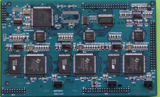
Now with the improvement of the IC process, the digital signal rising edge time is also "passively" shorter, previously only need to consider the line to pull through the PCB, more and more need to take into account the transmission line effect when wiring, in order to better guide the electromagnetic wave, to avoid signal integrity problems and in line with EMC performance, and single-layer or double-layer board, For the current IC integration and wiring density, it is difficult to have space to construct a good transmission line structure, which requires the use of four-layer boards, or even six-layer boards, the key signals rich in high harmonics are transmitted by strip lines.
With the development of semiconductor technology, we have to consider the use of multi-layer boards to construct transmission lines for electromagnetic wave guidance. For the 6-layer board, basically there will be BGA or QFN chip, SMT on the surface of the PCB flatness requirements, the surface of the solder pad flat, conducive to welding, and high density high layer board is perfect fit. The use of disc hole technology can also save the surface wiring space occupied by the fan hole, further improve the wiring density of the surface layer, in addition, the use of disc hole technology makes the power/ground pad can be directly connected to the main power/ground plane through the hole, avoiding the influence of the lead parasitic inductance of the fan hole, which is also helpful for the integrity of the power supply.
kinhford Electronics is a professional PCB design company engaged in electronic product circuit board design (layout layout design), mainly undertake multi-layer, high-density PCB design and circuit board design proofing business. With an average of more than 10 years of work experience in PCB design team, can skillfully use the market mainstream PCB design software, professional and efficient communication to ensure PCB design progress, to help you seize the market opportunity one step earlier!


Just upload Gerber files, BOM files and design files, and the KINGFORD team will provide a complete quotation within 24h.