
Professional PCB manufacturing and assembly
Building 6, Zone 3, Yuekang Road,Bao'an District, Shenzhen, China
+86-13410863085Mon.-Sat.08:00-20:00

There are three basic signal grounding methods: floating ground, single point ground, and multi-point ground.
1 Floating purpose: to isolate the circuit or equipment from the public wire that may cause circulation, floating also makes it easy to cooperate between circuits with different potentials. Disadvantages: electrostatic accumulation is easy to cause strong electrostatic discharge. Compromise: Access the bleed resistor.
2 Single-point grounding: Only one physical point in the line is defined as the grounding reference point, and all the points that need to be grounded are connected to this point. Disadvantages: Not suitable for high frequency applications.
3 Multi-point grounding mode: The point that needs to be grounded is directly connected to the ground plane nearest to it, so that the grounding cable length is shortest. Cons: More difficult to maintain.
4 Hybrid grounding Select single point and multi-point grounding as required.
The large-area copper ground in the PCB is actually multi-point ground, so single-sided Pcb can also achieve multi-point ground
The increase of multi-layer PCB is mostly a high-speed circuit layer, which can effectively improve the electromagnetic compatibility of PCB is the basic means to improve signal anti-interference, and also due to the mutual isolation of the power layer and the bottom layer and different signal layers, the cloth flux of PCB also increases the interference between signals.

PCB circuit board production process introduction
PCB production process is more complex, it involves a wide range of processes, from simple machining to complex machining, there are ordinary chemical reactions and photochemical electrochemical thermochemistry and other processes, computer-aided design CAM and other aspects of knowledge. Moreover, in the production process, there are many process problems and new problems will be encountered from time to time, and some problems will disappear without finding out the cause. Because the production process is a non-continuous form of assembly line, any problem in any link will cause the whole line to stop production or a large number of scrapped consequences. If the printed circuit board is scrapped, it can not be recycled. The job of process engineer is stressful, so many engineers leave the industry to work in sales and technical services for PCB equipment or materials manufacturers.
The substrate of the board itself is made of an insulating, non-bendable material. The small wire material that can be seen on the surface is copper foil. Originally, the copper foil is covered on the whole board, and the middle part is etched away during the manufacturing process, and the remaining part becomes a network of small lines. These lines are called conductors (conductor pattern) or wiring, and are used to provide circuit connections for parts on the PCB.
To secure the parts to the PCB, we solder their pins directly onto the wiring. On the most basic PCB (single panel), the parts are concentrated on one side, and the wires are concentrated on the other side. In this way, we need to make holes in the board, so that the connector can pass through the board to the other side, so the connector of the part is welded to the other side. Because of this, the front and back sides of the PCB are called Component Side and Solder Side, respectively.
If there are some parts on the PCB that need to be removed or put back after production, then the Socket will be used when the part is installed. Since the socket is welded directly on the board, the parts can be arbitrarily disassembled.
If you want to connect two PCBS to each other, generally we will use the edge connector commonly known as "golden finger". The gold finger contains many exposed copper pads, which are actually part of the PCB wiring. Usually, when connecting, we insert the gold finger on one PCB into the appropriate Slot on the other PCB (generally called expansion Slot). In computers, such as video cards, sound cards and other similar interface cards, are connected to the main board by the goldfinger.
The green or brown on the PCB is the solder mask color. This layer is an insulating protective layer that protects the copper wire and also prevents parts from being welded to incorrect places. A silk screen is printed on top of the solder mask. It is usually printed with text and symbols (mostly white) to indicate the position of the parts on the board. Screen printing surface is also called legend surface.
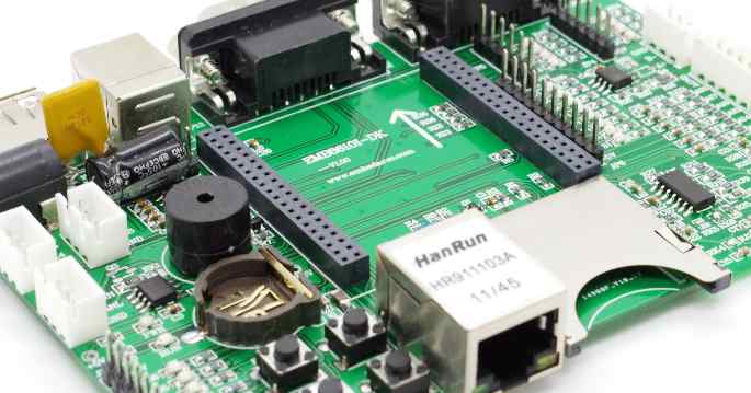
Printed circuit board The complex circuit copper wire between parts and parts is etched on a board after careful and neat planning, providing the main support body for the installation and interconnection of electronic components, and is an indispensable basic part of all electronic products.
Printed circuit board A flat plate made of a non-conductive material, usually with a design pre-drilled for mounting chips and other electronic components. The holes of the components help to connect the pre-defined metal paths printed on the surface of the board electronically. After the pins of the electronic components are passed through the PCB, a conductive metal electrode is attached to the PCB to form a circuit.
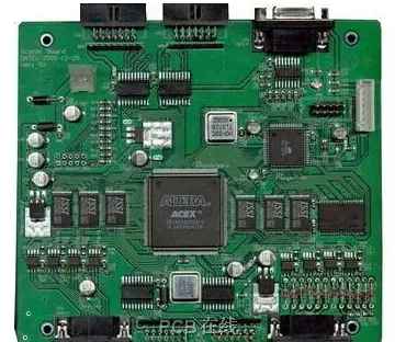
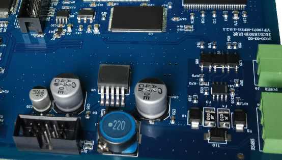
According to its application field PCB can be divided into single panel, double panel, more than four layers of multi-layer board and soft board. In general, the more complex the function of the electronic product, the longer the loop distance, the more the number of contact pins, the more the number of layers required by the PCB, such as high-level consumer electronics, information and communication products; The soft board is mainly used in products that need to be bent: such as notebook computers, cameras, automotive instruments, etc.


Just upload Gerber files, BOM files and design files, and the KINGFORD team will provide a complete quotation within 24h.