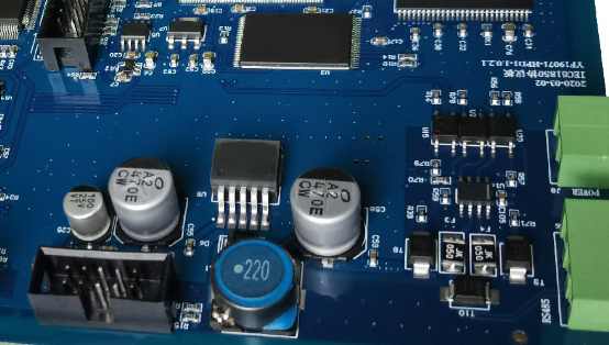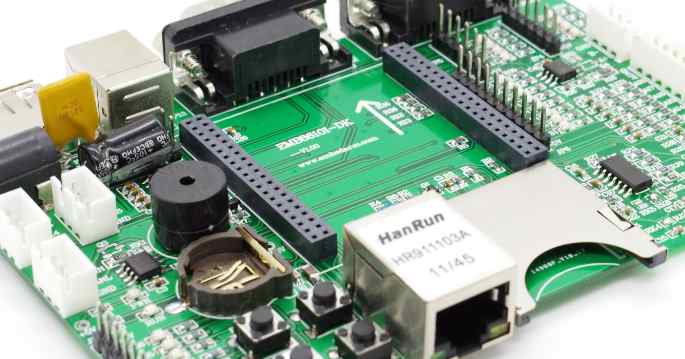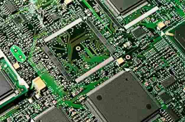
The 3-day 2015 International Circuit Board and electronic Assembly South China Exhibition was held in Shenzhen Convention and Exhibition Center on the 2nd, and more than 500 companies from around the world participated in this industry event.
According to reports, the exhibition is co-sponsored by the Hong Kong Circuit Board Association and the International Electronics Industry Association. Relying on the distribution role of the industry bridgehead in Shenzhen, the exhibition has developed into the world's largest circuit board and electronic assembly industry exhibition since its inception in 2002. The exhibition area of this exhibition reached 50,000 square meters, the number of booths more than 2,500, basically covering the entire supply chain of circuit boards and electronic assembly. In order to cater to the "Industry 4.0" boom, the exhibition specially added the "Intelligent automation Zone" and the "Intelligent automation Future Development exhibition area of the circuit board industry", and the application of a large number of robotic arms and CNC automatic equipment greatly improved the efficiency of the printed circuit board production process. In the environmental protection and clean zone, a number of innovative technologies and solutions applied to the "three wastes" (waste gas, wastewater, solid waste) treatment and resource recovery in the printed circuit board industry were also displayed.

Ms. Li, general manager of Shenzhen Hongyunlai Electronic Technology Co., LTD., who participated in the exhibition, believes that the current copper clad plate is still the main material for the production of printed circuit boards, and the large use of this basic product makes the environmental protection pressure of the industry remain high. With the increasing attention of the country to environmental protection, there is a huge market demand in the printed circuit board industry in the field of wastewater treatment and recovery, etching liquid copper recovery, microcorrosion waste liquid recovery, nitric acid waste liquid recovery and treatment.
Analysis of the rules of PCB Layout 3W20H55
The 3W Principle:
3W is the distance between the lines to stay 3 times the line width. You said 3H would do. But here the H is the line width. Not the thickness of the medium. In order to reduce crosstalk between lines, it should be ensured that the line spacing is large enough, if the line center distance is not less than 3 times the line width, 70% of the electric field between lines can be maintained without interfering with each other, which is called the 3W rule. If 98% of the electric fields do not interfere with each other, the 10W rule can be used.
20H Principle:
20H refers to the distance between the power layer and the formation, which is also to suppress the edge radiation effect. The edge of the plate radiates electromagnetic interference. The power layer is shrunk so that the electric field is conducted only within the range of the ground layer. Effectively improve EMC. If the retraction is 20H, 70% of the electric field can be limited within the grounding edge. Retraction for 100H can contain 98% of the electric field.
Five -- five rules:
Printed board layer selection rule, that is, clock frequency to 5MHz or pulse rise time is less than 5ns, PCB board must use multi-layer board, this is a general rule, sometimes for cost and other factors, the use of double-layer board structure, in this case, it is best to use one side of the printed board as a complete ground plane layer.
EMC
Electromagnetic compatibility (EMC) is the ability of a device or system to operate as required in its electromagnetic environment without creating intolerable electromagnetic interference to any equipment in its environment. Therefore, EMC includes two requirements: On the one hand, it means that the electromagnetic interference generated by the equipment in the normal operation of the environment cannot exceed a certain limit; On the other hand, it means that the appliance has a certain degree of immunity to electromagnetic interference in the environment, that is, electromagnetic sensitivity.
Electromagnetic sensitivity refers to any electromagnetic phenomenon that degrades the performance of a device or system. The so-called electromagnetic interference refers to the deterioration of the performance of the equipment or system caused by electromagnetic interference. Traditionally, EMC includes EMI (Electromagnetic interference) and EMS (electromagnetic sensitivity).
EMS (Electro Magnetic Susceptibility) electromagnetic sensitivity, which refers to the ease of performance degradation due to electromagnetic energy.
EMI(Electro Magnetic Interference) Electromagnetic interference, including conduction, radiation, and harmonics.
Electromagnetic Compatibility (EMC) Electromagnetic compatibility
EMC=EMI+EMS
The 20H principle in PCB design:
The "20H rule "is used to ensure that the edge of the power plane is retracted at least 20 times as much as the layer distance between the two planes as the edge of the 0V plane. This rule is often required as a technique for reducing side-shot emission from 0V/ power plane structures (suppressing edge radiation effects). However, the 20H rule provides significant benefits only under certain conditions. These specific conditions include:
1. The rise/fall time of current fluctuation in the power bus is less than 1ns.
2. The power plane should be on the internal level of the PCB, and the upper and lower levels adjacent to it are 0V planes. The two 0V planes should extend outward at a distance equal to at least 20 times the distance between their respective layers and the power plane.
3. The power bus structure does not generate resonance at any frequency of concern.
4. The total derivative of the PCB is at least 8 layers or more.


