
Professional PCB manufacturing and assembly
Building 6, Zone 3, Yuekang Road,Bao'an District, Shenzhen, China
+86-13410863085Mon.-Sat.08:00-20:00

What mistakes are often made during PCB design?
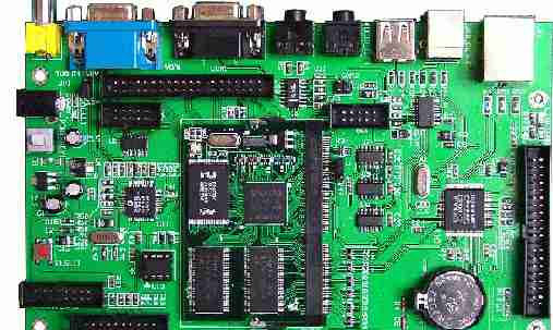
PCB design is a very critical part of electronic product manufacturing. Its quality is directly related to the performance and stability of the entire product. However, in the process of designing PCB, many people will make some common mistakes, which if not corrected in time, will greatly affect the quality of the product. This article will analyze these mistakes that are often made in the PCB design process, and hope to provide you with some helpful suggestions.
Mistake 1: PCB size design is not reasonable
When designing a PCB, first determine the size of the PCB. If the PCB size design is unreasonable, it will not only lead to an increase in PCB manufacturing costs, but also affect the stability and reliability of the circuit. Therefore, when carrying out PCB size design, it is necessary to carry out reasonable design according to the actual situation of electronic products to avoid wasting circuit space.
Error 2: The PCB line is going into chaos
In terms of PCB circuit design, the mistake that many people are prone to make is that the line goes to chaos, which not only increases the difficulty of wiring, but also makes the performance of the PCB unstable. Therefore, when PCB circuit design is carried out, it is necessary to route in accordance with the circuit schematic diagram, and try to make the line concise and clear. Mistake 3: Not taking electromagnetic compatibility into account
In PCB design, electromagnetic compatibility is a very critical issue. If the PCB design does not meet the requirements of electromagnetic compatibility, it will cause electromagnetic interference, affecting the performance and stability of the circuit. Therefore, in the PCB design process, we must fully consider electromagnetic compatibility, reasonable circuit protection of the PCB, reduce the impact of electromagnetic interference, and ensure the normal operation of the product.
Mistake 4: Not doing a rigorous rule check
Before the PCB design, be sure to carry out a strict rule check. The contents of the inspection include PCB size, line direction, electromagnetic compatibility and so on. Only after the rules are checked, can the subsequent PCB design work be carried out. Otherwise, there may be various problems in the subsequent work, affecting the quality of the entire electronic product.
Mistake # 5: Using the wrong PCB material
In the PCB design process, choosing the right PCB material is also very critical. The use of inappropriate PCB materials will affect the performance and stability of the PCB, and even make the entire electronic product unable to operate normally. Therefore, in the PCB design, it is necessary to choose the PCB material that meets the requirements to ensure the normal operation of the circuit.
Mistake # 6: Not doing enough testing and validation
After the PCB design is completed, it is necessary to carry out adequate testing and verification of the PCB. Only after testing and verification can the PCB be used in actual electronic products. Otherwise, it may cause the circuit performance to be unstable or even unable to operate normally because of some problems left over in the design process. In short, in the PCB design process, we must pay attention to the above frequently made mistakes, timely discovery and correction. Only in this way, under the premise of ensuring the quality of PCB, can we produce electronic products with high stability and excellent performance.
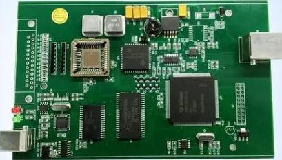
SMT or surface mount technology is one of the most commonly used technologies in modern electronics production. It has been widely used in various fields, including automotive electronics, consumer electronics, industrial automation and so on. In the SMT patch processing process, there are some key considerations that we need to pay special attention to.
First of all, for each step of SMT patch processing, we need to ensure that the operator has been professionally trained and mastered the correct operating methods and processes. In the product assembly, welding and testing links, each link needs professional technology and strict operation process. Only in this way can we guarantee the quality of the patch products.") https://www.kingfordpcb.com/yuan.php
https://www.kingfordpcb.com/yuan.php
Secondly, we need to pay attention to the materials and requirements of SMT patches. The materials required for SMT patch processing are very important, such as the printed circuit board (PCB), components, solder, etc., that the patch needs to use. For different types of patches, we need to choose appropriate materials, and process and test according to requirements.
Third, patch processing requires very strict quality inspection procedures. We need to conduct a comprehensive inspection of each batch of products to ensure that the performance and quality of the products meet the requirements. In SMT chip processing, we need to fully monitor and manage the welding process, assembly process, testing process and other aspects. Only in this way can we guarantee the stability and reliability of our products.
In addition, in the SMT patch processing process, we also need to pay attention to details. For example, when collaging components, it is necessary to carefully check whether the label and position of the components are accurate. In the welding process, it is necessary to ensure the quality of welding, but also need to pay attention to the rationality of welding parameters. In addition, we also need to ensure the accuracy of various materials and documents of the patch to ensure that the final quality of the product meets the requirements.
In short, SMT patch processing is a very complex and meticulous process. In the entire process of processing, we need to pay attention to quality, materials and quality inspection, pay special attention to every detail, to ensure that products reach the highest level of quality standards. Only in this way can we meet the needs of the market and contribute to the development of the electronics industry.


Just upload Gerber files, BOM files and design files, and the KINGFORD team will provide a complete quotation within 24h.