
Professional PCB manufacturing and assembly
Building 6, Zone 3, Yuekang Road,Bao'an District, Shenzhen, China
+86-13410863085Mon.-Sat.08:00-20:00

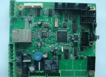
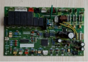
Notice and operation skills of circuit board design
1. The definition of processing level should be clear
When there is no clear place in the document, be sure to find a professional engineer to check, so as to reduce the chance of plate making errors.
2, the distance between the copper foil and the outer frame can not be too close
Large area of copper foil from the outer frame distance to maintain at least 0.2 mm spacing.
3. Do not use filler blocks to draw welding pads
Drawing pad with filler block is OK in circuit board design, but it can not be used in processing, because such pad can not directly generate solder resistance.
4, the ") https://www.kingfordpcb.com/yuan.php?time=1685377305can not flower welding pad and line coexistence
https://www.kingfordpcb.com/yuan.php?time=1685377305can not flower welding pad and line coexistence
The ground is different from the actual printed plate image, they are opposite, all the lines are barrier lines, can not leave a gap, otherwise it is easy to lead to short circuit of the power supply.
5. The pad should not be too short
If the pad is too short, it is easy to misposition the test pin. Because of the dense pad, the spacing between the feet is very small, and the pad is very thin. When installing the test needle, it must be staggered up and down to complete, otherwise this situation will occur.6, the pad can not overlap
Pad overlap is easy to lead to scrap phenomenon in the drilling process, so the pad must not overlap. Notice and operation skills of circuit board design
1. The definition of processing level should be clear
When there is no clear place in the document, be sure to find a professional engineer to check, so as to reduce the chance of plate making errors.
2, the distance between the copper foil and the outer frame can not be too close
Large area of copper foil from the outer frame distance to maintain at least 0.2 mm spacing.
3. Do not use filler blocks to draw welding pads
Drawing pad with filler block is OK in circuit board design, but it can not be used in processing, because such pad can not directly generate solder resistance.
4, the electric formation can not flower welding pad and line coexistence
The ground is different from the actual printed plate image, they are opposite, all the lines are barrier lines, can not leave a gap, otherwise it is easy to lead to short circuit of the power supply.
5. The pad should not be too short
If the pad is too short, it is easy to misposition the test pin. Because of the dense pad, the spacing between the feet is very small, and the pad is very thin. When installing the test needle, it must be staggered up and down to complete, otherwise this situation will occur.
6, the pad can not overlap
Pad overlap is easy to lead to scrap phenomenon in the drilling process, so the pad must not overlap. The main function of the steel mesh is to assist in the deposition of solder paste, with the aim of transferring the exact amount of solder paste to the exact location on the empty PCB. In SMT patch processing, it is used to ration solder paste or patch glue, which is the key tool to ensure the printed circuit board. According to the characteristics of the process and the material, thickness, size of the different, the charging standard of steel mesh is usually about one hundred to seven hundred yuan, how to choose according to the requirements of customer design and comprehensive consideration of the process.
Usually, when the pin spacing is more than 0.025in, chemical etching template is selected to achieve the same printing effect as other technologies. When the pcb board pin spacing is less than 0.020in, laser cut and electrocast formwork should be considered. Another technique to improve paste release for spacing below 0.020in is a trapezoidal section opening with the flare down.


Just upload Gerber files, BOM files and design files, and the KINGFORD team will provide a complete quotation within 24h.