
Professional PCB manufacturing and assembly
Building 6, Zone 3, Yuekang Road,Bao'an District, Shenzhen, China
+86-13410863085Mon.-Sat.08:00-20:00


Avionics are inevitably subjected to vibration and shock in the process of production, transportation and use. The effects of these vibrations and shocks can lead to many forms of failure or even destruction of electronic equipment. These vibration and impact caused by the damage of electronic equipment screw and nut loose, chassis deformation, PCB solder joint fracture peeling, device pin fracture, etc. Especially with the continuous development of PCB to the direction of high precision, high density, small spacing, multi-layer, high-speed transmission and the rapid development of VLSI, its function is more complete, the volume is smaller, package more pins, more dense IC and SOIC, especially the wide application of surface mount technology (SMT). All of them pose higher challenges to PCB components.

For avionics equipment, the failure caused by vibration and shock will greatly reduce its reliability and have extremely serious consequences. The relevant literature shows that the failure rate of avionics products caused by vibration and impact dynamic environment accounts for 28.7% of the total failure rate. PCB also occurs frequently in the vibration environment test of avionics equipment. Through dynamic analysis and design of PCB components, the probability of failure in environmental tests can be reduced effectively, and the reliability and quality of avionics products can be improved.
Dynamic analysis is based on the analysis of dynamic characteristics. The dynamic model of PCB component can be established by analyzing its dynamic characteristics. Only by establishing accurate dynamic model can dynamic analysis be carried out effectively. Therefore, this paper attempts to use the finite element analysis (FEA) and experimental modal analysis (EMA) to analyze the dynamic characteristics of a PCB component of avionics equipment, and establish the finite element dynamic analysis model of the PCB component.
1. Finite element modal analysis
As a mature numerical analysis technique, finite element analysis (FEA) is widely used to analyze the dynamic characteristics of PCB components of electronic equipment. In addition, FEAs can help engineers design more reliable PCB components by predicting potential failure and fatigue from the beginning of design. In this paper, the PCB component of an avionics equipment (FIG. 1) is taken as the research object. Its dimensions (length × width × thickness) are 133.5mm×79mm×1.8mm, which is fixed on the casing of the electronic equipment by screws at four corners of the PCB. The PCB component is similar to the standard test PCB, but the thickness is larger. Components and connectors are assembled by surface mount technology (SMT) and PCB, among which the packaging of components is mainly BGA, QFP and SOP.
1.1 Finite element analysis model
Table 1 shows the physical performance parameters of the materials that make up each part of an object PCB component. According to the PCB component geometry information and related material information, the finite element analysis model was established in ANSYS (Figure 2). Since the dynamic performance data of PCB components as a whole is to be obtained, rather than the detailed data of components themselves, components and connectors are simplified when building the model. Specifically, rectangular and square blocks are used to simulate components, and connectors are used to simulate their rough appearance. Each part of the finite element analysis model adopts three-dimensional solid unit (SOLID187) for grid division (using solid unit for grid division, although it increases the calculation amount to a certain extent, but the workload from CAD to CAE model is greatly reduced, which is conducive to engineering application and promotion). The connections between components and PCB and connectors and PCB are simulated by multi-point constraint (MPC). At the same time, because the stiffness of the electronic housing is much greater than that of the PCB component, the finite element model imposes a fixed support constraint on the screw holes at four corners to simulate the screw connection between the PCB component and the equipment housing.
1.2 Results of finite element modal analysis
The finite element model of PCB module was established and modal analysis was carried out by Block Lanczos Method. Modal analysis is to obtain the eigenvalues and eigenvectors of the system by solving the characteristic equations of the system. The characteristic equations of the general multi-degree-of-freedom system can be expressed in the form shown in Equation (1), namely, the natural frequencies and mode shapes of the vibration system.
Where, [M]- mass matrix of the system, assembled from element mass matrix in finite element modal analysis; [K]- the stiffness matrix of the system, assembled from the element stiffness matrix in the finite element modal analysis; {X} - displacement vector of the system; Omega - the eigenvalue of the system.
Through modal analysis, the first three natural frequencies and mode shapes of the PCB module fixed with four screws are obtained. The first mode mode of the PCB component is first order bending, the second mode mode is torsion, and the third mode mode is sine-wave bending. These modes are similar to those obtained for the JEDEC standard plate fixed with four screws.

SMT plant production management
May 27,2023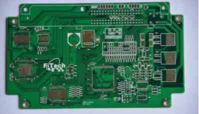


Just upload Gerber files, BOM files and design files, and the KINGFORD team will provide a complete quotation within 24h.