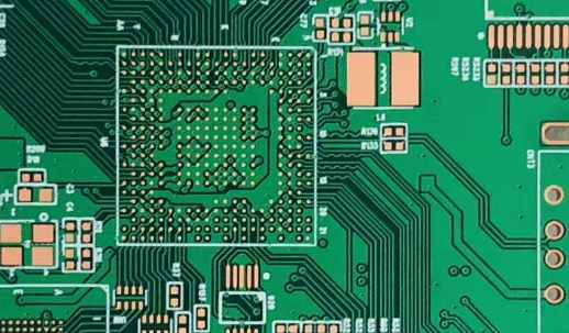
Curing is a key process in the patch glue - wave soldering process. In many cases, due to poor curing or incomplete curing of the patch glue, especially the uneven distribution of components on PCB, components will fall off in the process of transportation and welding. Therefore, it is very important to do a good job of curing.
For PCB, two kinds of curing methods are commonly used, one is thermal curing, the other is uv curing; Epoxy patch adhesive adopts thermal curing. The early thermal curing was carried out in the oven. Now, it is mostly cured in the infrared reflow furnace to realize continuous production. Before the formal production should first adjust the furnace temperature, make the furnace temperature curing curve of the corresponding product, do more attention to the curing curve is: different manufacturers, different batch number of patch adhesive curing curve will not be exactly the same; Even if the same patch glue, used in different products, because of the size of the board, the number of components, the set temperature will be different, this point is often ignored. It is often the case that when welding IC devices, after curing, all the pins still fall on the pad, but after wave soldering, the IC pins will shift or even leave the pad and produce welding defects. Therefore, to ensure the quality of welding, we should adhere to the temperature curve of each product, and we should do it carefully. In the curing process, two important parameters should be paid attention to: one is the initial temperature rise rate; Second, the peak temperature. The temperature rise rate determines the surface quality after curing, while the peak temperature determines the bonding strength after curing. These two parameters should be provided by the patch supplier, which is more meaningful than the curing curve provided by the supplier. It can give you an idea of the properties of the patch used.

The test method of curing curve of patch glue in infrared reflow furnace and the instrument used are the same as the method of infrared reflow furnace temperature curve of solder paste. The heating rate and curing furnace temperature curve can be designed according to the parameters provided by the supplier. In case of disputes, in addition to negotiating with suppliers, differential scanning thermal analysis (DSC) can be carried out in the relevant testing department to identify adhesive properties.
When the light curing adhesive is used, the reflow furnace with UV light is used for curing, the curing speed is fast and the quality is high. At present, for PCB curing, the most suitable use or UV light source, because UV light source has the characteristics of other mercury lamps do not have, just take the light source, UV light source is a cold light source, the curing principle is that the light irradiation of the glue under the action of the photocatalyst reaction, finally curing. Cold light curing does not occur because hot PCB elements are affected. Say another characteristic of UV light source - curing fast, fast to what extent, can complete curing in 1 second, in the production method can be said to be curing industry to improve work efficiency of a kind of irreplaceable equipment. On these two characteristics, UV light source is fully qualified to replace the traditional light source, of course, and green environmental protection, energy saving and other advantages. Overall, UV light source is or will be the most suitable light source for PCB photocuring.
Rogers High frequency plate factory opened to support the upgrading of China's 3G/4G industry
Rogers Corporation recently held a ground-breaking ceremony for its Advanced Circuit Materials Division (ACM Division) in Suzhou Industrial Park.
ACM is one of the core business units of Rogers. Its main products are high-frequency printed circuit board materials, which are widely used in communication base stations, radio frequency antennas, satellite receivers and other industries. The new facility was completed in 2010 and started production in 2011, with a total investment of more than US $20 million. It will significantly increase the global manufacturing capacity of ACM Division to meet the growing market and customer needs. The factory will be fully operational in the third quarter of 2011, providing material technology support for the upgrading and rapid development of 3G/4G communication industry in the Chinese market.
Rogers is a company with a long history. Since its founding in Connecticut in 1832, the company started from the paper industry and has developed into a global leader in the research and development and production of special materials and products through continuous innovation and product and market diversification. Rogers Technology (Suzhou) Co., Ltd. was established in Suzhou Industrial Park in June 2002 with a registered capital of US $20 million and a total investment of US $55 million. Now it has 6 business units and more than 800 employees. The company has four plants put into use, stainless steel water tank total construction area of about 50,000 square meters. At the same time, the company is expanding its seven sales offices in Asia, which are located in Korea, Japan, Singapore, Taiwan and Shanghai, Beijing and Shenzhen in mainland China. In 2010, Rogers' sales in Asia accounted for more than 50% of its global sales. The company is committed to developing strategic markets and management localization in China and Asia to create a first-class company run by a professional and outstanding team in China.


