
Professional PCB manufacturing and assembly
Building 6, Zone 3, Yuekang Road,Bao'an District, Shenzhen, China
+86-13410863085Mon.-Sat.08:00-20:00


Circuit boardnames are: circuit board, PCB board, aluminum substrate, high frequency plate, thick copper plate, impedance board, printing (copper etching technology) circuit board, etc. The circuit board makes the circuit miniaturized and intuitive, which plays an important role in the mass production of fixed circuit and the optimization of electrical appliance layout. And PCB welding resistance blistering is a problem that many PCB factories inevitably appear in the processing of PCB, so what causes the welding resistance blistering? The following is for you to sort out the introduction:
1. Poor pretreatment (uneven brush grinding on the surface of the circuit board, residual water stains, oil stains), if the surface treatment of the circuit board is not good, it is easy to lead to welding resistance of the circuit board.
2, copper surface sag: there are many kinds of circuit board boards, generally international boards will not appear copper foil sag phenomenon, some circuit board users in order to reduce the cost of pcb circuit board manufacturers to use a relatively low price circuit board, when the solder resistance printing to the concave position will produce adhesion decline, so will produce solder resistance off phenomenon.

3. Multiple spraying tin or the temperature of the tin pot is too high: multiple spraying tin or the temperature is too high will affect the adhesion of the circuit board welding resistance. Welding resistance has a certain high temperature resistance, but once it exceeds its range, it will affect the adhesion of welding resistance, so it leads to welding resistance foaming.
4. Uneven ink thickness: in the welding resistance of printed circuit board, especially when printing by hand, there will often be different thickness of welding resistance printing. Therefore, where the welding resistance is relatively thick, the adhesion of welding resistance decreases due to insufficient drying time, which will lead to welding resistance foaming.
The signal layers are distributed between the solid reference plane layers, and they can be symmetrical or asymmetric strip lines. A 12 - layer board is taken as an example to illustrate the structure and layout of multi - layer board. Its layered structure is T-p-s-p-s-p-s-s-p-b, with "T" as the top layer, "P" as the reference plane layer, "S" as the signal layer and "B" as the bottom layer. From the top layer to the bottom layer, the first layer, the second layer,?? The 12th floor. The top and bottom layers are used as pads for the components, and signals should not be transmitted over long distances at the top and bottom layers in order to reduce direct radiation from the wiring. Incompatible signal lines should be isolated from each other in order to avoid coupling interference between them. High frequency and low frequency, large current and small current, digital and analog signal lines are incompatible, component layout should put the incompatible components in different positions on the printed board, in the layout of signal lines should still pay attention to isolate them.
The following three questions should be paid attention to when designing:
(1) Determine which reference plane layer will contain multiple power supply areas for different DC voltages. Assuming that layer 11 has multiple DC voltages means that the designer must keep the high-speed signal as far away from layer 10 and layer 10 as possible, since the return current cannot flow through the reference plane above layer 10 and needs to use the stitched capacitance. Layers 3, 5, 7 and 9 are the signal layers of the high-speed signal, respectively. The routing of important signals should be arranged in one direction as much as possible to optimize the number of possible routing channels on the layer. The signal routes distributed on different layers should be perpendicular to each other, which can reduce the coupling interference of electric and magnetic fields between the lines. The third and seventh layers can be set as "east-west" routes, while the fifth and ninth layers are set as "north-south" routes. The layer of the cable cloth should be based on the direction of its destination.
(2) The change of layers when high-speed signals are routed, and which different layers are used for an independent routing to ensure that the return current flows from one reference plane to the new reference plane required. This is to reduce the area of the signal loop and the differential mode and common mode current radiation of the loop. Loop radiation is proportional to current intensity and loop area. In fact, the best design does not require the return current to change the reference plane, but simply to change from one side of the reference plane to the other. For example, combinations of signal layers can be used as signal layer pairs: Layer 3 and 5, Layer 5 and layer 7, Layer 7 and layer 9, which allows an east-west direction and north-south direction to form a wiring combination. However, the combination of layers 3 and 9 should not be used because it requires the return current to flow from layer 4 to Layer 8. Although a decoupling capacitor can be placed near the through-hole, it is rendered useless at high frequencies by the presence of leads and through-hole inductors. In addition, this kind of routing will increase the area of signal loop, which is unfavorable to reduce the current radiation.
(3) Select the DC voltage for the reference plane layer. In this example, due to the high speed of signal processing inside the processor, there is a lot of noise on the power/ground reference pin. Therefore, it is important to use decoupling capacitors in providing the same DC voltage to the processor, and to use them as efficiently as possible. The best way to reduce the inductance of these components is to make the wiring as short and wide as possible, and to make the through-hole as short and thick as possible.

What costs will pcba OEM involve
May 22,2023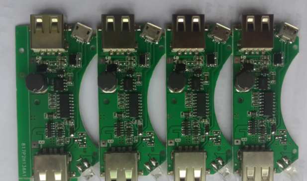


Just upload Gerber files, BOM files and design files, and the KINGFORD team will provide a complete quotation within 24h.