
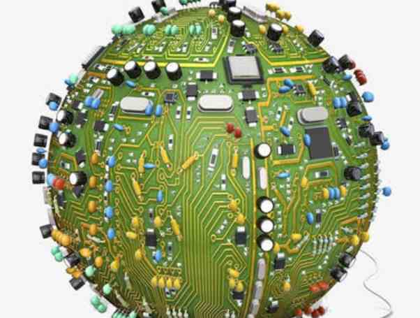
Professional PCB manufacturing and assembly
Building 6, Zone 3, Yuekang Road,Bao'an District, Shenzhen, China
+86-13410863085Mon.-Sat.08:00-20:00

In the case of the PCB board technology and the number of circuits have been decided, the next is to decide the size of the PCB board. If the design is too large, then the packaging technology will have to change, or re-split the action. The quality and speed of the diagram should also be taken into account when selecting the technology. Using SMT is cheaper than using THT because the PCB board will have more dense (and smaller) components.
If the PCB board is densely packed with components, the wiring must be finer and the equipment used must be of a higher order. At the same time, the material used should also be more advanced, and the design of the wire must be more careful, so as not to cause power consumption and other problems affecting the circuit. These problems cost more than the savings from reducing the size of PCB boards.
More layers of PCB boards cost more, but fewer layers of PCB boards usually result in an increase in size. PCB embedded holes are more expensive than pilot holes that run through all layers. Because burials have to be drilled before they can be joined. The size of the hole on the PCB board is determined by the diameter of the pin of the part.
If the PCB board has different types of pin parts, then the machine can not use the same drill bit to drill all the holes, the relative time consumption, also represents a relative increase in manufacturing costs. Electronic tests using a flypin probe are usually more expensive than optical tests. Optical testing is generally sufficient to ensure that there are no errors on the PCB board.
Shenzhen Hongyunlai Electronics is a professional pcb circuit board factory, with advanced production equipment and perfect after-sales service system. Provides more information on pcb pcb design, pcb PCB proofing, single side/multilayer PCB PCB fabrication, smt patch processing.
Third, PCB design copper foil thickness, wire width and current relationship

The current strength of the signal. When the average current of the signal is large, the current carried by the wiring width should be considered. The line width can refer to the following data:
PCB design copper foil thickness, wire width and current relationship
The carrying capacity of copper foil of different thickness and width is shown in the following table:
PCB design copper platinum thickness, line width and current relationship
Note:
i. When copper wire is used to pass through high current, the carrying capacity of copper foil width should be selected and considered by referring to the value derating by 50% in the table.
ii. In PCB design and processing, OZ is commonly used as the unit of copper skin thickness. 1 OZ copper thickness is defined as the weight of copper foil within 1 square foot area is 1 ounce, and the corresponding physical thickness is 35um; 2OZ copper thickness 70um.
Comply with 12 principles, SMT patch processing is 0 bad
The following are 12 principles of zero defect of SMT patch processing by Hongyunlai Electronic Finishing company. If you abide by these principles, you can ensure zero defect of SMT patch processing to the maximum extent.
1, the principle of full inspection: all parts and products must be fully inspected.
2. The principle of inspection in the process: quality is manufactured, so it must be inspected in the process.
3. The principle of stopping the line: Once a defect is found in the process, the person who understands it needs to stop the production line (behavior) immediately and start to eliminate the countermeasures.
4, the principle of responsibility: the operator of bad process, must immediately do the repair or repair, determine everyone's scope of responsibility.
5. The principle of arresting active criminals: once bad things happen, when and by whom, on which machine and with what materials, they should be able to confirm immediately, rather than using the mentality of imagining suspects.
6. The principle of thorough implementation of standard operations: Standard operations refer to the operator's operations that are regular and repetitive in each cycle, and must be checked in each cycle.
7, the principle of all paths to the same destination: reduce working hours, so that potential defects can be shown, and then reduce defective products, while improving productivity and quality level.
8, N=2 inspection principle: if in the process of automatic machine batch production, the inspection of the first product and the last product of each batch is equal to the principle of full inspection, this principle is also applicable in the thorough implementation of standardization and production line stability.
9, the principle of error prevention device: to prevent bad occurrence, can not completely rely on the attention of the operator, and must prevent the wrong device to prevent human negligence and error.
10, check the task principle: not to do the selection, but to eliminate the poor because of the effort of the object.
11, the principle of no complaints: to completely and thoroughly manage the quality, to zero bad as the goal, to provide zero bad goods to customers.
12, the principle of single flow: to complete a product, immediately carry out the next process, that is, single flow means, this is the basic method of early detection of bad, and reduce handling, storage, waiting, so the chance of bad occurrence will be reduced.
Shenzhen Hongyunlai Electronic Technology Co., LTD., to give you the best quality SMT patch processing,PCB production, embedded system research and development, electronic processing, embedded motherboard,PCBA contract materials, Guangzhou PCBA processing services.


Just upload Gerber files, BOM files and design files, and the KINGFORD team will provide a complete quotation within 24h.