
Professional PCB manufacturing and assembly
Building 6, Zone 3, Yuekang Road,Bao'an District, Shenzhen, China
+86-13410863085Mon.-Sat.08:00-20:00

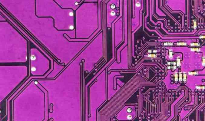
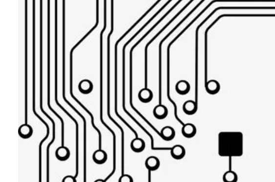
Through hole (via) is one of the important components of multilayer PCB, the cost of drilling usually accounts for 30% to 40% of the PCB board. Simply put, every hole in the PCB can be called a pass hole.
In terms of function, pores can be divided into two categories:
One is used as an electrical connection between the layers;
The second is used for fixing or positioning devices.
In terms of PCB board manufacturing process, these holes are generally divided into three categories, namely blind via, buried via and through via.
Blind holes are located on the top and bottom surfaces of the PCB and are of a certain depth. They are used to connect the surface circuit to the inner circuit below. The depth of the holes usually does not exceed a certain ratio (aperture).
Buried holes are connection holes located in the inner layer of the PCB that do not extend to the surface of the PCB. Both types of holes are located in the inner layer of the circuit board, which is completed by a through-hole molding process prior to lamination. Several inner layers may be overlapped during the through-hole formation process.
Through hole. This hole runs through the entire circuit board and can be used for internal interconnection or as a positioning hole for component installation. Because the through hole in PCB board process is easier to realize, the cost is lower, so the vast majority of printed circuit boards are using it, rather than the other two through holes.
The following mentioned through holes, without special instructions, are considered as through holes. From the design point of view, a through hole is mainly composed of two parts, one is the drill hole in the middle, and the other is the welding pad area around the drill hole.
The size of these two parts determines the size of the hole. Obviously, in the design of high speed, high density PCB, the designer always wants the hole as small as possible, the template can leave more wiring space, in addition, the hole is smaller, its own parasitic capacitance is smaller, more suitable for high speed circuit. But as hole sizes get smaller, they cost more, and don't keep getting smaller. They're limited by PCB plating and drilling techniques such as drill and plating. The smaller the holes, the longer it takes to drill, and the more likely they are to be off-center at their plating. When the hole depth is more than 6 times the diameter of the hole, it is impossible to guarantee the uniform copper plating on the hole wall. For example, the thickness (through hole depth) of a normal 6-layer PCB board is about 50Mil, so the minimum drilling diameter provided by PCB manufacturers can only reach 8Mil.

Parasitic capacitance through the hole itself has parasitic capacitance to the ground. If the diameter of the isolation hole through the hole on the paving layer is D2, the diameter of the welding plate through the hole is D1, the thickness of the PCB board is T, and the dielectric constant of the substrate is ε, the parasitic capacitance through the hole is approximately: C= 1.4epsilon TD1/(D2-D1) The main effect of the parasitic capacitance through the hole on the circuit is to prolong the signal rise time and reduce the speed of the circuit.
For example, for a PCB board with a thickness of 50Mil, if a through-hole with an inner diameter of 10Mil, a diameter of 20Mil of the pad is used, and the distance between the pad and the copper floor area is 32Mil, then we can approximate the parasitic capacitance of the through-hole through the above formula: C=1.41x4.4x0.050x0.020/(0.032-0.020)=0.517pF, the rise time change caused by this part of capacitance is: T10-90=2.2C(Z0/2)=2.2x0.517x(55/2)=31.28ps.
It can be seen from these values that although the effect of the parasitic capacitance of a single hole is not obvious, the designer should be careful if multiple holes are used to switch between layers in the route.
Vii. How to meet EMC requirements as far as possible without causing too much cost pressure?
The increased cost caused by EMC on PCB board is usually caused by increasing the number of layers to enhance shielding effect and increasing ferrite bead and choke to inhibit high frequency harmonic devices. In addition, it is usually necessary to match the shielding structure on other organizations to make the entire system pass EMC requirements.
The following are just a few tips for PCB board design to reduce the electromagnetic radiation effects generated by circuits.
1. When possible, use devices with slow signal slope (slew rate) to reduce slew components.
2. Pay attention to the position of the high-frequency device, do not be too close to the external connector.
3. Pay attention to impedance matching of high-speed signals, routing layer and return current path, so as to reduce high-frequency reflection and radiation.
4. Place enough and appropriate de-coupling capacitors in the power pins of each device to mitigate the noise on the power layer and the ground. Pay special attention to whether the frequency response and temperature characteristics of the capacitor meet the design requirements.
5. The ground near the external connector can be properly separated from the ground, and the ground of the connector is connected to the chassis ground.
6, can be appropriate to use the ground guard/shunt traces in some special high-speed signals. However, pay attention to the influence of guard/shunt traces on the characteristic impedance of the line.
7. The power layer is 20H smaller than the inside of the formation, and H is the distance between the power layer and the formation.
Eight, when a PCB board has multiple number/mode function blocks, the conventional practice is to separate the number/mode, why?
The reason for separating digital/mode ground is that digital circuit will produce noise in the power supply and ground when switching between high and low potential, and the noise size is related to the signal speed and current size. If the ground plane is not divided and the noise generated by the circuit in the digital region is large and the circuit in the analog region is very close, the analog signal will still be disturbed by the ground noise even if the digital-analog signal does not cross. That is to say, the digital-to-analog undivided way can only be used when the analog circuit area is far away from the digital circuit area that generates large noise.


Just upload Gerber files, BOM files and design files, and the KINGFORD team will provide a complete quotation within 24h.