
Professional PCB manufacturing and assembly
Building 6, Zone 3, Yuekang Road,Bao'an District, Shenzhen, China
+86-13410863085Mon.-Sat.08:00-20:00

In the PCB cloning process, after the board copy is completed, the exported PCB file diagram is sent to the board factory for board manufacturing. There are many technical materials involved in the process of copying the board, but there are few detailed systematic descriptions of the process of making the board. Here, Shenzhen Honglijie professional board technician according to their own experience, to explore the whole process of PCB board.
First, the preliminary project
After getting the PCB file drawing, it is necessary to check and analyze the file drawing, review the effect of the file drawing and related materials, and make full preparation, so as to ensure that there is enough available information in the subsequent process to carry out various processing determination, avoid delay in the project progress and mistakes and rework.
Two, medium system plate
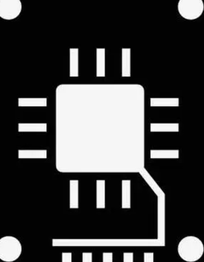
In the formal board making process, it is necessary to distinguish the dual panel from the multi-panel.
1, double panel system board
The first step is to cut the board. The size of the PCB board is determined by the related parameters of the file diagram.
The second step, CNC drilling, hole size according to the diameter of the parts to determine the size of the pin
The third step, the hole metallization, is to paint the pilot hole with metal so that it can connect the wires on both sides
The fourth step, the graphic transfer, the PCB printed circuit graphic transfer to the copper coated plate, commonly used screen leakage method and photochemical method.
The fifth step, check and repair, remove the debris in the hole, because the resin epoxy will produce some chemical changes after heating, so it needs to be removed first.
The sixth step is line plating, that is, coating the surface of the line with a layer of copper.
The seventh step, etching, involves dipping the board into an etching solvent or spraying the solvent onto the board.
The eighth step is to remove the film, that is, to remove the remaining photoresist.
2, multi-panel board
The first step, again, is to cut the board, only for multiple panels, the board is relatively thin, because the overlap of multiple panels must ensure that the resulting PCB board can meet the requirements of its application.
The second step, drill the positioning hole, the inner pattern
The third step, the inner layer etching, defilm
The fourth step, blackening, is a coarse treatment for the copper surface, the purpose is to make the copper surface of the multilayer plate and the resin sheet can maintain strong solid force after pressing.
The fifth step, lamination, multilayer plate must be each single plate pressed together, add insulation layer between the layers, and each other firmly.
The sixth step, CNC drilling
Step seven, outer graphics
The eighth step, as with the double panel, check and repair, line plating, etching, defilm and so on.
Three, the late process
In this process, dual panels follow the same rules as multiple panels.
1, silk screen welding and character, electric gold-plated fingers
First, cover the outermost wiring with solder resistance paint. This ensures that the wiring does not touch beyond the plating section. The screen printing surface is then printed on it to mark the position of each part. Shenzhen Honglijie reminds plate makers that the gold finger part is usually plated with gold to ensure high quality current connection.
2, hot air leveling, PCB board surface treatment.
3, slot, that is, to add an expansion slot on the board.
4. Power-up test to detect whether there is short circuit or short circuit phenomenon of PCB. Shenzhen Honglijie usually uses flying needle detector for electrical test, which can ensure high accuracy.
5. The final inspection, according to PCB file drawing and other board making requirements, to carry out comprehensive inspection of performance and quality.
6. Shipping. After the PCB board is shipped from the board factory, the parts can be installed and welded to further complete the board assembly.
Manual wiring is an important process in PCB design now and in the future. Using manual wiring helps automatic wiring tools to complete the wiring work.
By routing and fixing the selected network manually, a path can be formed for automatic routing.
First of all, key signals can be wired manually or combined with automatic wiring tools. After the wiring is completed, the relevant engineering and technical personnel will check the signal wiring. After the check is passed, the wires will be fixed, and then the rest of the signals will be automatically wired.

Because of the existence of impedance in ground wire, common impedance interference will be brought to the circuit. Therefore, when wiring, do not connect any point with ground symbol, which may produce harmful coupling, affect the work of the circuit.
At higher frequencies, the inductive reactance of the wire will be several orders of magnitude greater than the resistance of the wire itself. At this time, even if only a small high frequency current flows through the wire, there will be a certain high frequency voltage drop. Therefore, for high frequency circuits, the PCB layout is as compact as possible so that the printed wires are as short as possible.
There are mutual inductance and capacitance between printed wires. When the working frequency is large, it will cause interference to other parts, which is called parasitic coupling interference. The suppression methods that can be adopted are:
Minimize signal routing between levels;
Arrange all levels of circuits in the order of signals to avoid crossing each other's signal lines;
The wires of the adjacent two panels should be vertical or cross, not parallel;
When the signal wires are arranged in parallel in the board, the wires should be separated as far as possible by a certain distance, or the ground line, the power line, to achieve the purpose of shielding.

Share PCB board hole making technology
May 19,2023


Just upload Gerber files, BOM files and design files, and the KINGFORD team will provide a complete quotation within 24h.