
Professional PCB manufacturing and assembly
Building 6, Zone 3, Yuekang Road,Bao'an District, Shenzhen, China
+86-13410863085Mon.-Sat.08:00-20:00

Printed circuit boards, also known as printed circuit boards, are providers of electrical connections for electronic components. Printed circuit boards are often expressed as "PCB", but not called "PCB board". It has a history of more than 100 years; Its design is mainly layout design; The main advantage of using circuit board is to greatly reduce wiring and assembly errors, improve the level of automation and production labor rate. Next, let me tell you about the history of pcb circuit board. What categories does it fall into?
What is the history of pcb circuit board?
Step 1: History
(1) Before the appearance of printed circuit boards, the interconnection between electronic components is to rely on wires directly connected to form a complete circuit. In modern times, circuit panels exist only as effective experimental tools, while printed circuit boards have become the absolute dominant position in the electronic industry.
(2) At the beginning of the 20th century, in order to simplify the production of electronic machines, reduce wiring between electronic parts, reduce production costs and other advantages, so people began to study the method of printing to replace wiring. For thirty years, engineers have proposed adding metal conductors to the insulated substrate as wiring. The most successful was in 1925, Charles Ducas of the United States printed circuit patterns on insulated substrate, and then successfully built conductors as wiring by electroplating.
(3) It was not until 1936 that Paul Eisler, an Austrian, published foil film technology in Britain, using printed circuit boards inside a radio unit; In Japan, palace this pleased help to spray the attached wiring method "メ タ リ コ ン blowing wiring method (chartered 119384)" success to apply for a patent. Of the two, Paul Eisler's method, which is most similar to today's printed circuit boards, is called subtracting, in which unwanted metal is removed. Charles Ducas and Kinosuke Miyamoto did this by adding only the wiring needed, called the addition method. However, because of the high heat of the electronic parts at that time, the substrate of the two was difficult to use together, so there was no formal practical use, but it also made the printed circuit technology further.
Step 2 Grow
(1) In recent ten years, the Printed Circuit Board (PCB) manufacturing industry has developed rapidly in our country. The total output value and total output rank first in the world. As electronic products change rapidly and price wars change the structure of the supply chain, China has become the world's most important production base for printed circuit boards with industrial distribution, cost and market advantages.
(2) The printed circuit board has developed from single layer to double panel, multilayer board and flexible board, and has continuously developed to the direction of high precision, high density and high reliability. Constantly reduce the size, reduce the cost, improve the performance, so that the printed circuit board in the future of the development of electronic products, still maintain strong vitality.
(3) The development trend of PCB manufacturing technology in the future is to develop in the direction of high density, high precision, fine aperture, fine wire, small spacing, high reliability, multi-layer, high-speed transmission, light weight and thin shape.
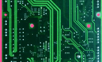
Two, pcb into which categories?
1. Single panel
On the most basic PCB, the parts are concentrated on one side and the wires on the other. Because wires appear on only one side, this type of PCB is called Single-sided. Only early circuits used such boards because a single panel had many severe limitations on the design circuit (because there was only one side, the wiring could not be crossed and had to be routed in a separate path).

2. Dual panel
Both sides of the circuit board have wiring, but to use the wires on both sides, there must be a proper circuit connection between the two sides. This "bridge" between circuits is called a pilot hole (via). A pilot hole is a small hole in a PCB filled with or coated with metal that can be connected to wires on both sides. Because the area of the dual panel is twice as large as that of the single panel, the dual panel solves the difficulty of the single panel due to the interleaving of the wiring (can be passed to the other side through the pilot), and it is more suitable for use in more complex circuits than the single panel.
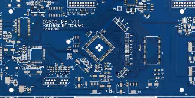
3. Multilayer board
In order to increase the area that can be wired, more single or double sided wiring boards are used in multilayer boards. A printed circuit board with a double-sided inner layer, two single-sided outer layer or two double-sided inner layer, two single-sided outer printed circuit board, through the positioning system and insulating binder materials alternately together and conductive graphics in accordance with the design requirements of the interconnection of the printed circuit board becomes a four-layer, six-layer printed circuit board, also known as the multilayer printed circuit board. The number of layers of the board does not mean that there are several independent wiring layers. In special cases, empty layers will be added to control the thickness of the board.
Usually, the number of layers is even and includes the outermost two layers. Most of the main board is a 4 to 8 layer structure, but technically it is possible to achieve close to 100 layers of PCB. Most large supercomputers use quite a few layers of mainframe boards, but because such machines can be replaced by clusters of ordinary computers, super-multiboards have fallen out of use. Because the layers in the PCB are so tightly integrated, it is not always easy to see the actual number, but if you look closely at the main board, you can see it.
The above is my "What is the history of pcb circuit board? What categories does it fall into?" The introduction, for your reference, I wish you a happy life!


Just upload Gerber files, BOM files and design files, and the KINGFORD team will provide a complete quotation within 24h.