
Professional PCB manufacturing and assembly
Building 6, Zone 3, Yuekang Road,Bao'an District, Shenzhen, China
+86-13410863085Mon.-Sat.08:00-20:00

China has long been a manufacturing power. In the field of PCB, with the overall trend of the global PCB industry transferring to Asia, China has already become the world's largest PCB producer. If you break it down even further, 18 years ago, the top three regions in terms of annual output value were Taiwan, Japan and then mainland China. But now 18 years of statistics out, according to statistics, mainland China has surpassed Japan to become the world's second largest PCB production region.
digitimes reported that according to Prismark statistics, Taiwan's total output value of PCBS in 2018 was $62.4 billion, accounting for 31.3% of the world's largest market share, while the Chinese mainland accounted for 23%, surpassing Japan's 20% market share to become the world's second largest PCB-producing region.
In addition, as of the end of 2018, 13 of the world's top 30 PCB manufacturers are from Taiwan, and 5 of the top 10 are from Taiwan. They are Zhen Ding Technology, Xin Xing Electronics, Huatong Computer, Jian Ding Technology and Hanyu Bode. These manufacturers work in slightly different areas of PCB application, and their customers are mostly first-tier brand suppliers in different areas.
While only three of the top 30 -- Dongshan Precision, Shennan Circuit and Jingwang Electronics -- are from the Chinese mainland, they all posted significant revenue growth this year.
Among them, Zhen Ding Technology, the world's largest PCB maker, has widened its gap with second place Japan's Qisheng to more than $1 billion. Zhen Ding is currently a leader in flexible circuit boards and baseboard-like PCB (SLP) technology, and has also completed the deployment of rigid and flexible bonded boards, IC substrates and COF substrates.
Xinxing Electronics and Huatong Computer, both of which have deep deployments in PCBS for mobile phones and consumer electronics, saw their 2018 revenue fall sharply due to poor sales in the end-consumer market.
On the mainland side, Dongshan Precision has generated more than $1 billion in revenue in two years by acquiring Mflex, a U.S. manufacturer of FPCBS, and Multek, a Hong Kong PCB assembler. In addition, Shennan Circuit's revenue grew as much as 36 percent year on year in 2018, thanks to strong demand from major customers such as Huawei and ZTE for PCB shipments of 5G base stations.

In contrast, Japan's largest PCB maker Ichikatsu saw its revenue fall 14.4 percent year on year in 2018, mainly due to a decline in FPCB products. And, in fact, of Japan's major FPCBS manufacturers, only Fujikura posted positive growth in 2018.
Of the top five PCB manufacturers in Japan -- Nishikatsu, Fujikura, Ibiden, Meiko, and Sumitomo Denko -- with the exception of Meiko being the sole pure PCB manufacturer, all of them only manufacture PCBS as part of their business. They generally lag behind pure-play PCB makers in technology development and capacity expansion, and so are losing ground in the PCB space, as PCB manufacturing is an increasingly capital - and technology-intensive industry. But Japanese manufacturers are strong in supplying PCBS to their country's carmakers.
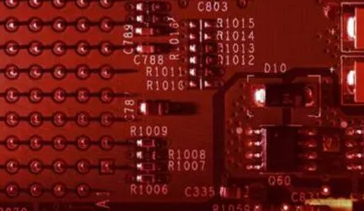
1, from the cost and signal quality, choose a reasonable size of the hole size. For example, for the design of 6-10 layers of memory module PCB, it is better to choose 10/20Mil (drill/pad) pass hole, for some high-density small size boards, you can also try to use 8/18Mil pass hole. With current technology, it is difficult to use smaller holes. For the power supply or ground wire hole can be considered to use a larger size, to reduce the impedance.
2. From the two formulas discussed above, it can be concluded that the use of thinner PCB board is beneficial to reduce the two parasitic parameters through the hole.
3. The signal routing on the PCB board should not be changed as far as possible, that is to say, try not to use unnecessary holes.
4. The pins of the power supply and the ground should be drilled nearby. The shorter the lead between the pins and the holes, the better, because they will lead to the increase of inductance. At the same time, power and ground leads should be as thick as possible to reduce impedance.
5. Place some grounded holes near the holes of the signal changing layer in order to provide the nearest loop for the signal. You can even put a lot of extra ground holes on the PCB board.


Just upload Gerber files, BOM files and design files, and the KINGFORD team will provide a complete quotation within 24h.