
Professional PCB manufacturing and assembly
Building 6, Zone 3, Yuekang Road,Bao'an District, Shenzhen, China
+86-13410863085Mon.-Sat.08:00-20:00


The output value of PCB(printed circuit board) industry is the largest industry in the subdivided industry of global electronic components. With the deepening of research and development and the continuous upgrading of technology, PCB products are gradually developing to the direction of high density, small aperture, large capacity, thin and light. In 2015 and 2016, the global output of PCB increased slightly, but the output value of PCB denominated in US dollar decreased slightly, influenced by the large depreciation of yen and euro compared with the US dollar and other factors. According to Prismark statistics, the total output value of the global PCB industry reached $62.4 billion in 2018, with a year-on-year growth of 6.0%. According to Prismark, the global PCB market will maintain moderate growth in the next two years, and the output value of PCB will reach $66.1 billion in 2020. The Internet of Things, automotive electronics, industry 4.0, cloud servers, storage devices, etc. will become the new direction driving the growth of PCB demand.
The PCB industry is widely distributed in the world. Developed countries in Europe and the United States started early, developed and made full use of advanced technology and equipment, so the PCB industry has achieved considerable development. In the past two decades, relying on the advantages of Asia, especially China, in labor, resources, policies, industrial clustering and other aspects, the global electronics manufacturing capacity has been transferred to China, Taiwan, South Korea and other Asian regions. With the shift of global industrial center to Asia, PCB industry presents a new pattern of manufacturing center in Asia, especially in mainland China. Since 2006, China has surpassed Japan and become the world's largest PCB producer, with both output and output value ranking first in the world. In recent years, the global economy has been in a period of deep adjustment, and the driving role of major economies such as Europe, the United States and Japan to world economic growth has been significantly weakened, and their PCB market has seen limited growth or even contraction. China is increasingly integrated with the global economy, and gradually occupies half of the global PCB market.
Note: SEA/ROW represents Southeast Asia/other countries and regions worldwide
As the largest producer of PCB industry in the world, China accounted for 52.4% of the total output value of the global PCB industry from 8.1% in 2000 to 52.4% in 2018. The output value of America, Europe and Japan declined sharply, while the PCB industry in mainland China and other parts of Asia (mainly South Korea, Taiwan and Southeast Asia) developed rapidly.

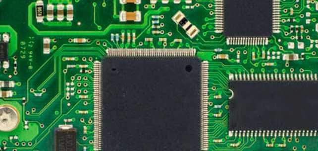
PCB board appears to throw copper factors
PCB is one of the indispensable parts of electronic equipment, it appears in almost every kind of electronic equipment, in addition to fixing a variety of large and small parts, the main function of PCB is to let the parts electrical connection. Since the raw material of PCB board is copper-covered board, copper dumping will occur in the process of PCB production. Then what are the reasons for copper dumping of PCB board? Prinlin Xiaobian below for everyone to introduce.
1, PCB circuit design is not reasonable, with thick copper foil design of too thin line, will also cause excessive line etching and copper.
2, copper foil etching is excessive, the electrolytic copper foil used on the market is generally single-side galvanized (commonly known as gray foil) and single-side plated copper (commonly known as red foil), the common copper is generally more than 70um galvanized copper foil, red foil and 18um below the basic ash foil has not been a batch of copper.
Baoneng is committed to providing customers with one-stop electronic components and PCB online procurement services, providing thousands of electronic components procurement, price inquiry and transaction, BOM BOM service, to ensure that all components are purchased from the original factory or agents formal channels, to ensure the original authentic, is a professional electronic components procurement website in China
3. Local collision occurs in PCB process, and the copper wire is separated from the substrate by external mechanical force. This defect manifests as poor positioning or orientation, falling copper wire will have obvious distortion, or in the same direction of the scratch/impact mark. Peel off the bad part of the copper wire to see the copper foil surface, you can see the normal color of the copper foil surface, there will be no bad side erosion, copper foil peeling strength is normal.
4. Under normal circumstances, as long as the hot pressing high temperature section of the laminate exceeds 30 minutes, the copper foil and the semi-cured sheet are basically combined completely, so the pressing generally will not affect the binding force of the copper foil and the substrate in the laminate. However, in the process of laminate stacking and stacking, if PP pollution or copper foil surface damage, it will also lead to insufficient bonding force between copper foil and substrate after laminate, resulting in positioning (only for the large plate) or sporadic copper wire loss, but the stripping strength of copper foil near the stripping line will not be abnormal.


Just upload Gerber files, BOM files and design files, and the KINGFORD team will provide a complete quotation within 24h.