
Professional PCB manufacturing and assembly
Building 6, Zone 3, Yuekang Road,Bao'an District, Shenzhen, China
+86-13410863085Mon.-Sat.08:00-20:00

Nowadays, the volume of switching power supply is getting smaller and smaller, and its working frequency and internal component density are getting higher and higher, which undoubtedly makes the anti-interference requirements of PCB layout of power supply more and more strict.
Power PCB design skills
First, component layout
The best way to establish a switching power supply layout is similar to its electrical design. The best design process is as follows:
1. Place the transformer
2. Design the power switch current circuit
3. Design the output rectifier current circuit
4. Connect the control circuit to the AC power supply circuit
5. Design the input current source loop and input filter
6. Design the output load loop and output filter
According to the functional unit of the circuit, the layout of all components of the circuit should comply with the following principles:
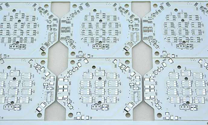
(1) The size of PCB should be considered first. When PCB size is too large, the printed line is long, the impedance increases, the anti-noise ability decreases, and the cost increases. Too small, the heat dissipation is not good, and the adjacent lines are susceptible to interference. The best shape of the circuit board is rectangular, the aspect ratio is 3:2 or 4:3, and the components located on the edge of the board are generally not less than 2mm away from the edge of the board.
(2) When placing the device, the future welding should be considered, not too intensive.
(3) Take the core component of each functional circuit as the center, and carry out the layout around it. The components should be arranged evenly, neatly and compact on the PCB, and the leads and connections between the components should be reduced and shortened as far as possible. The decoupling capacitor should be as close to the VCC of the device as possible.
(4) For circuits working at high frequency, distribution parameters between components should be considered. General circuits should be arranged as parallel as possible. In this way, not only beautiful, but also easy to assemble welding, easy to mass production.
(5) Arrange the position of each functional circuit unit according to the circuit flow, so that the layout is convenient for signal flow, and keep the signal in the same direction as far as possible.
(6) The first principle of layout is to ensure the distribution rate of wiring, mobile devices pay attention to the connection of the fly line, and put the connected devices together.
(7) Reduce the area of loop as much as possible to suppress the radiation interference of switching power supply.
Two, wiring
The switching power supply contains high-frequency signals, and any printed line on the PCB board can play the role of antenna. The length and width of the printed line will affect its impedance and inductive reactance, thus affecting the frequency response. Even printed lines that pass through the DC signal can couple from neighboring printed lines to the RF signal and cause circuit problems (or even re-radiate interference signals). All printed wires that pass through the AC current should therefore be designed to be as short and wide as possible, which means that all components connected to the printed wires and to other power lines must be placed close together.
The length of the printed line is proportional to its inductance and impedance, and the width is inversely proportional to the inductance and impedance of the printed line. The length reflects the wavelength of the printed line's response. The longer the length, the lower the frequency at which the printed line can send and receive electromagnetic waves, and the more radio-frequency energy it can radiate. According to the size of the printed circuit board current, try to rent the width of the power line, reduce the loop resistance. At the same time, the direction of the power cord and ground wire is consistent with the direction of the current, which helps to enhance the anti-noise ability.
(1) Wiring direction: from the perspective of welding surface, the arrangement orientation of components should be consistent with the schematic diagram as far as possible, and the wiring direction should be consistent with the wiring direction of the circuit diagram. Because various parameters are usually detected in the welding surface during the production process, it is convenient to do so for inspection, debugging and maintenance in the production (Note: On the premise of meeting the requirements of circuit performance, overall installation and panel layout).
(2) When designing the wiring diagram, try to minimize turning, the line width on the printing arc should not be sudden, the wire corner should be more than 90 degrees, and strive to make the line simple and clear.
(3) The printed circuit board is not allowed to have a cross circuit, for the possible cross lines, you can use "drill", "wind" two ways to solve. That is, let a lead from other resistance, capacitance, the gap at the foot of the audion "drill" in the past, or from the possible cross of a lead wire "around" in the past. In special cases if the circuit is very complex, in order to simplify the design also allow the use of wire jumper, to solve the problem of cross circuit.
(4) The input ground and the output ground in the switching power supply for low-voltage DC-DC, to feedback the output voltage back to the primary transformer, the circuit on both sides should have a common reference ground, so after the ground wire on both sides of the copper, but also connected together, to form a common ground.
PCB surface treatment process characteristics
Mar 17,2023


Just upload Gerber files, BOM files and design files, and the KINGFORD team will provide a complete quotation within 24h.