
Professional PCB manufacturing and assembly
Building 6, Zone 3, Yuekang Road,Bao'an District, Shenzhen, China
+86-13410863085Mon.-Sat.08:00-20:00

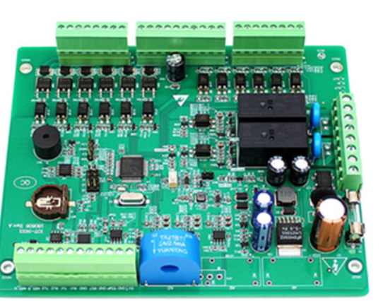
Shenzhen kingford is a professional manufacturer of printed circuit board manufacturing circuit board, for many years focused on single, double-sided, multi-layer circuit board production. Can provide impedance board, HDI board, blind hole plate and other multi-layer PCB board proofing, small batch production business, the following for you to analyze the factors affecting PCB price.
Factors affecting PCB price
First, PCB materials used in the diversity of prices
Take the common double panel for example, the board is generally fr-4, cem-3, plate thickness from 0.2mm to 5.0mm, copper thickness from 0.5oz to 3oz, all these in the board one item caused a huge price difference; In the welding ink, there is a certain price difference between ordinary thermosetting oil and photosensitive green oil, so the different materials cause the diversity of prices.
Second, the different production processes used by PCB result in the diversity of prices
Different production processes result in different costs. Such as gold-plated plate and spray tin plate, the production of shape gong (milling) plate and beer (punching) plate, the use of silk screen line and dry film line will form different costs, leading to the diversity of prices.
3. Price diversity caused by different difficulty of PCB itself
Even if the material is the same, the process is the same, but the difficulty of PCB itself will cause different costs. If there are 1000 holes on both types of circuit boards, the hole diameter of one board is greater than 0.6mm and that of the other board is less than 0.6mm, different drilling costs will be formed; If the other two kinds of circuit boards are the same, but the line width and line distance are different, one is greater than 0.2mm, one is less than 0.2mm, it will also cause different production costs, because the difficult board scrap rate is higher, the cost will increase, and then cause the diversity of price.
Four, different customer requirements will also cause different prices
The level of customer requirements will directly affect the finished product rate of the board factory, for example, a board according to ipc-a-600e, 98% qualified rate, but according to the class3 requirements may only 90% qualified rate, resulting in different costs of the board factory, and finally lead to the variable product price.
V. Price diversity caused by different PCB manufacturers
Even if the same product, but because of different manufacturers of process equipment, technical level is different, will form different costs, nowadays many manufacturers like to produce spray tin plate, because the process is simple, low cost, but also some manufacturers produce gold plate, scrap rate rises, resulting in higher costs, so they would rather produce spray tin plate, so their spray tin plate quotation is lower than the gold plate.
Vi. Price differences caused by different payment methods
At present, PCB board manufacturers generally adjust PCB prices according to different payment methods, ranging from 5%-10%, which also causes the difference in price.
7. Regional differences lead to price diversity
At present, in terms of geographical location in China, prices are increasing from south to north, and there are certain differences in prices in different regions, so regional differences also cause the diversity of prices.

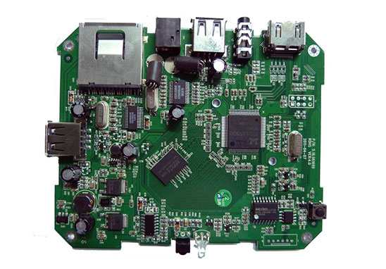
Difference between reflow welding and wave soldering in 2PCBA processing
In PCBA processing, two common welding methods are reflow welding and wave soldering. So in PCBA processing, what is the role of reflow welding, what is the role of wave soldering, and what is the difference between them? Next, Shenzhen PCBA processing manufacturer -kingford to introduce the difference between reflow welding and wave welding in PCBA processing.
The main difference between reflow welding and crest welding in PCBA processing is that crest welding is mainly used to weld plug-in components, while reflow welding is mainly used to weld patch components. The specific differences are as follows:
I. SMT reflow welding process
Reflow welding is simply used in chip component patches, referred to as smt patches. It is by first printing solder paste on the PCB pad, and then pasting machine to paste components on the pad printed with solder paste. The paste is then melted through a reflow furnace, then cooled and solidified. A process in which the welding end or pin of a component is connected to a PCB pad and energized. Reflow welding for short.
SMT products have the advantages of compact structure, small size, vibration resistance, impact resistance, high frequency characteristics and high production efficiency. SMT reflow welding has already occupied a position in PCB mounting process.
2. DIP crest welding process
Crest welding is simply the welding method of plug-in materials, referred to as DIP welding. Its technological requirements are to insert the plug-in material into the corresponding welding hole, and then through the furnace fixture, the circuit board into the pre-melted soft brazing furnace, the melted solder, through the mechanical pump or electromagnetic pump jet to form the solder crest, the solder joint through the crest will melt into the pore tin solder paste, after cooling solidification first plug-in material pin and through the hole welding, To achieve electrical performance. Short for: wave welding.
At present, the co-existence of reflow welding and wave welding is common in the design of intelligent products, which is also a starting point for smt SMT processing requirements of mixed assembly process. Both processes are available in SMT patch manufacturers.
Shenzhen kingford PCB board making ability
Number of layers: 2-40
Plate thickness: 0.2-7.0mm
Maximum copper thickness: 7oz
Finished product size: 650*1100mm
Minimum line width/spacing: 3/3mil
Maximum plate thickness aperture ratio: 12:1
Minimum mechanical drill diameter: 6mil
Hole to conductor distance: 3.5mil
Impedance tolerance (Ω) : ±5%(< 50) ±10%(≥50)
Surface treatment process: OSP, chemical gold plating, chemical nickel palladium gold, tin plating, silver plating, lead-free spray tin, hard gold plating, soft gold plating, gold finger, etc
Materials: FR-4, high TG, halogen-free, high frequency (Rogers, Isola...) , CEM, etc
Our advantages:
PCB board making service started in 1998, with fast delivery ability and quality assurance, can produce high level board, high TG board, HDI board, FPC, rigid torsion board, metal substrate and so on.
Delivery date of PCB allegro and sample:
Double-sided allegro can be completed in 24 hours, multi-layer allegro can be completed in 2-5 days;
Single/double-sided (0.6-1.6mm FR4) delivery time: 3-4 days;
Four-layer plate (0.6-1.6mm FR4) delivery time: 5-6 days;
Six-layer plate (0.8-1.6mm FR4) Delivery time: 7-8 days.
Market PCB enterprise
Mar 14,2023


Just upload Gerber files, BOM files and design files, and the KINGFORD team will provide a complete quotation within 24h.