
Professional PCB manufacturing and assembly
Building 6, Zone 3, Yuekang Road,Bao'an District, Shenzhen, China
+86-13410863085Mon.-Sat.08:00-20:00

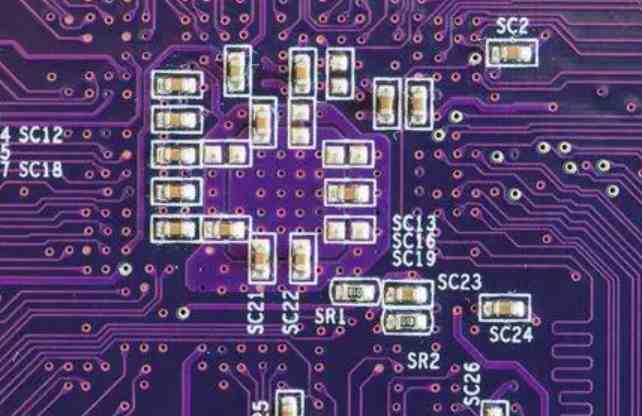
Overview of the application of phosphorus copper ball in PCB
1, phosphorus copper ball used in one of the PCB board copper and copper again process, the key depends on the generation of buried hole conductive copper layer
Two layers of PCB board products, because different layers of the middle of the route is not immediately connected, it is necessary to penetrate the structure of the buried hole to connect the middle of the different template layer route, easy to transfer polarity.
In the soldering tin of PCB board, after the route making of inner multilayer board, multi-layer pressing and mechanical equipment turning holes, in order to make the turning holes open and open, it is necessary to carry out the procedures of removing rubber slag, removing hair and organic chemical copper, and convert it into a thin copper layer. Then, through the titanium electrode rolling plating method to carry out the first and second rolling plating, improve the thickness of the copper layer to enhance the actual effect of the conductivity of the guide hole. Phosphorus copper ball is an important raw material for primary copper and secondary copper.

2, phosphorus copper ball for PCB rolling soldering anodic oxidation raw materials, phosphorus in the copper ball to avoid the harm of cuprous plating a thin layer of film quality
Phosphorous copper ball plays the role of anodic oxidation in PCB plating process tank, so phosphorous copper ball is also called anode copper ball. When the titanium electrode reaction starts, the copper molecules in the phosphorus copper ball will throw electronic devices and produce copper ions. The positively charged copper ions will move to the PCB board where the cathode is to be plated, and finally obtain electronic devices on the surface of the PCB board and convert into copper film.
In basic theory, phosphorus does not participate in the reaction of PCB plate rolling plating, and the key point of adding phosphorus depends on the dissolution rate of copper molecules. If the dissociation rate of copper molecules is too fast, there will be a lot of cuprous ions, and the two cuprous ions will reflect each other into copper molecules and copper ions. The copper molecules in the water solution will be adsorbed arbitrarily on the PCB board by the method of electrophoresis, which will harm the conversion of the copper coating into the structure and degrade the quality of the copper coating.
PCB does not need to use phosphorus containing copper ball _ phosphorus copper ball in PCB application overview
Phosphorous copper ball worldwide sales market forecast
1. The development trend of PCB board manufacturers moving to the mainland will not change, and the main performance of phosphorus copper ball is mainly in the mainland sales market.
The annual output value of PCB in mainland China has increased rapidly from 8.5% in 2000 to 25.2% in 2019. Due to the growing trend of PCB board products moving to the Mainland for manufacturing, the total value of PCB in the Mainland has reached the first place in the world.
It is estimated that the global sales market of phosphorus copper balls will increase from 146,501 tons in 2003 to 192,988 tons in 2008, with a CAGR of 5.7% (03-08). Among all regions, the mainland region showed the best performance, with a CAGR of 10.1% (03-08).
2. In the past, the phosphorus copper ball is mainly drawn by American and Japanese manufacturers. After the successful selection of the Taiwan plant, the existing two companies appear
Phosphorus copper ball harm PCB quality is very great, the previous choice of this industry companies include Mitsubishi, Asaba; American IMC, UniverTIcal and Germany Outokumpu.
In recent years, because the Asia-Pacific region has been a major manufacturing area of PCB board, Taiwan and mainland China have also invested in the development and burning of phosphorus copper ball products. The current development trend of more successful manufacturers include China's Taiwan Dong Youyue and mainland Xijiang electronic Devices. The two manufacturers have leapfrogged other investors to become the world's top two in terms of sales reported by the manufacturers.
PCB schematic design and process
Circuit schematic design is mainly the use of protel98 or protel99se schematic design system (Advanc sweet sehematic-) to draw a circuit schematic, which is the basis of the entire circuit design. In this process, we should make full use of various drawing tools and editing functions provided by Protel 98. The design process is as follows.
1. Start. Protel 98 circuit schematic editor
Potel 98 is started by clicking the Start icon in the Windows taskbar and selecting the Protel 98 command from the Programs menu.
2. Set the size and layout of the circuit drawing
Users can set the drawing size, direction, grid size and title bar.
3. Place components required for design on the drawing
According to the needs of the actual circuit, the user takes out the required components from the component library and puts them on the working plane, and adjusts and modizes the positions of the components.
4. Lay out and wire the components placed
The devices on the working plane are connected with wires and symbols of electrical significance to form a complete circuit schematic.
5. Adjust the components after the layout and wiring
In order to ensure that the schematic diagram is beautiful and correct, it is necessary to readjust the element position. Wire position to delete, move, change graphic size, attributes and arrangement.
6. Save the document and print it out
The circuit schematic design is saved or printed out by printer.


Just upload Gerber files, BOM files and design files, and the KINGFORD team will provide a complete quotation within 24h.