
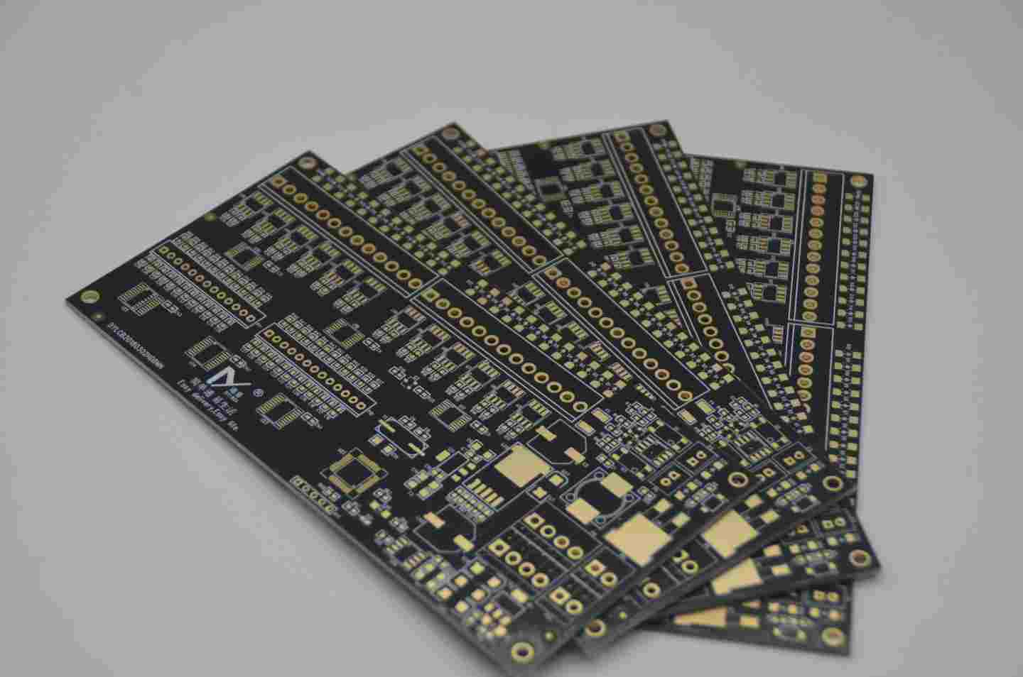
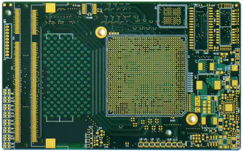
Professional PCB manufacturing and assembly
Building 6, Zone 3, Yuekang Road,Bao'an District, Shenzhen, China
+86-13410863085Mon.-Sat.08:00-20:00

As the proverb goes, "If a man has no plan, he will find trouble. "This of course also applies to the design of expedited PCB proofing. One of the many steps that can make a PCB design a success is choosing the right tools. Today's PCB design engineer can find many powerful and easy-to-use EDA kits on the market. Each has its own unique capabilities, advantages and limitations. It should also be noted that no piece of software is foolproof, so problems such as component packaging mismatches are bound to occur. While it may be possible that no single tool will meet all your needs, you must do some research beforehand and try to find the best product for your needs.
Poor communication While outsourcing PCB board design to other vendors is becoming more common and often very cost-effective, this practice may not be appropriate for complex PCB board designs, where performance and reliability are critical. As design complexity increases, face-to-face communication between engineers and expedited PCB proofing designers becomes important to ensure accurate component layout and wiring in real time. This face-to-face communication can help save costly rework later.
It is also important to invite PCB manufacturers early in the design process. They can provide initial feedback on your design, and they can maximize efficiency based on their processes and procedures, which will save you considerable time and money in the long run. By letting them know your design goals and inviting them to participate in the early stages of PCB layout, you can avoid any potential problems before the product is in production and shorten time to market.
Failing to thoroughly test an early prototype board will allow you to prove that your design is working according to the original specifications. Prototype testing allows you to verify the functionality and quality of PCB boards and their performance prior to mass production. Successful prototype testing takes a lot of time and experience, but a strong test plan with a clear set of goals can shorten the evaluation time and also reduce the likelihood of production-related errors. If any problems are found during prototype testing, a second test is performed on a reconfigured circuit board. By incorporating high risk factors early in the design process, you will benefit from multiple iterations of testing to identify any potential problems early, mitigate risks, and ensure that the plan is on schedule.
Smaller, faster devices that use inefficient layout techniques or incorrect components force PCB design engineers to lay out complex designs that will use smaller components to reduce footprint, and they will be placed closer together. Adopting technologies such as embedded discrete devices on the internal PCB layer, or ball-grid array (BGA) packages with smaller pin spacing will help reduce board size, improve performance, and preserve space that can be redone if problems are encountered.
When used with components with a high number of pins and smaller spacing, it is important to select the correct circuit board layout technique at design time so as to avoid problems later and minimize manufacturing costs. In addition, it is important to carefully study the value range and performance characteristics of the replacement components you intend to use, even those labeled as drop-in replacements. Small changes in the characteristics of replacement components can be enough to mess up the performance of the entire design.
Circuit board EMI standard
Feb 19,2023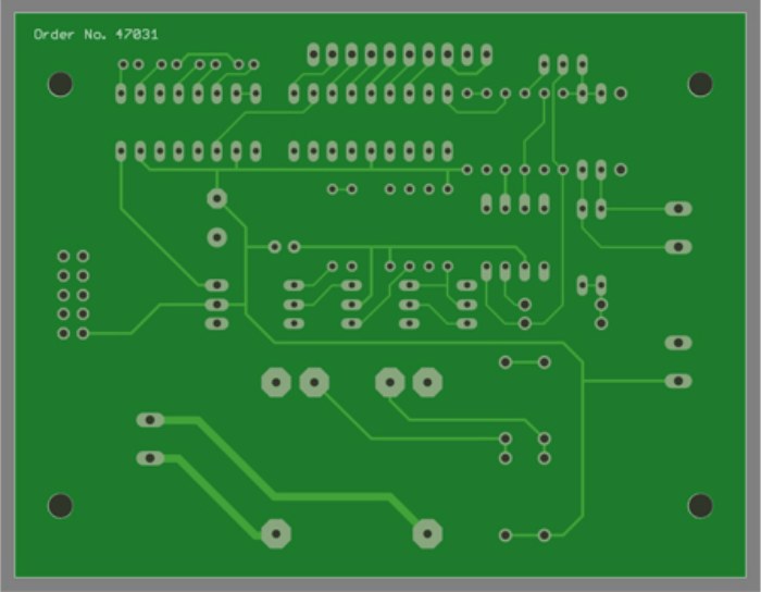


Just upload Gerber files, BOM files and design files, and the KINGFORD team will provide a complete quotation within 24h.