
Professional PCB manufacturing and assembly
Building 6, Zone 3, Yuekang Road,Bao'an District, Shenzhen, China
+86-13410863085Mon.-Sat.08:00-20:00

The frequency of electronic signals and processors of electronic equipment is increasing continuously. Electronic system has become a complex equipment containing many components and many subsystems. High density and high speed will increase the radiation of the system, while low pressure and high sensitivity will reduce the immunity of the system. Therefore, electromagnetic interference (EMI) is a threat to the safety, reliability and stability of electronic equipment. When we design electronic products, the design of PCB circuit board is very important to solve EMI problems. This article mainly explains the PCB design should pay attention to, so as to reduce the electromagnetic interference problem in PCB board.
Definition of electromagnetic interference (EMI)
EMI (Electro Magnetic Interference) can be divided into radiation and conduction interference. Radiation interference is the interference source uses space as a medium to interfere its signal to another electrical network. The conduction interference is to use the conductive medium as a medium to interfere with the signal of one electric network to another electric network. In high-speed system design, integrated circuit pins, high frequency signal lines and all kinds of plugs are common sources of radiation interference in PCB circuit board design. The electromagnetic wave they emit is electromagnetic interference (EMI), which will affect the normal work of themselves and other systems.
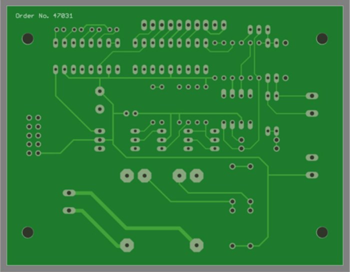
Design techniques of PCB circuit boards for Electromagnetic interference (EMI)
Nowadays, there are many solutions to EMI problems in circuit board design techniques, such as EMI suppression coating, suitable EMI suppression parts and EMI simulation design.
Tip 1: common-mode EMI interference sources (such as the transient voltage formed at the busbar of the power supply and the voltage drop formed at both ends of the inductance of the decoupling path)
1. When low value inductors are used in the power layer, the transient signals synthesized by inductors will be reduced, thus reducing common mode EMI.
2. Reduce the cable length between the power layer and the IC power pin.
3. Use 3-6 mil PCB layer spacing and FR4 dielectric material.
Tip two: electromagnetic shielding
1. Place the signal wires on the same PCB layer as far as possible and close to the power layer or grounding layer.
2. The power layer should be as close to the grounding layer as possible
Skill three: the layout of parts (different layout will affect the interference and anti-interference ability of the circuit)
1. According to different functions in the circuit for block processing (such as demodulation circuit, high-frequency amplifier circuit and mixing circuit, etc.), in this process to separate the strong and weak electrical signals, digital and analog signal circuits should be separated
2. The filtering network of each part of the circuit must be connected nearby, which can not only reduce the radiation, so as to improve the anti-interference ability of the circuit and reduce the chance of interference.
3. Avoid interference sources, such as CPU interference on the data processing board, in the layout of easily interfered parts.
Tip four: wiring considerations (unreasonable wiring will cause cross interference between signal lines)
1. Do not route the wires close to the frame of the PCB circuit board, so as not to break the wires during production.
2. The power cord should be wide so that the loop resistance will be reduced.
3. The signal cable should be as short as possible and the number of holes should be reduced.
4 Corner wiring can not be used right Angle method, should be 135° Angle is preferable.
5. Digital circuit and analog circuit should be isolated with ground wire, digital ground wire and analog ground wire should be separated, and finally connected to the power supply
Reducing electromagnetic interference is an important part of PCB board design, as long as the design to think more about this side, naturally in the product test such as EMC test will be easier to pass.
Black PCB board must be high-end board
Feb 19,2023


Just upload Gerber files, BOM files and design files, and the KINGFORD team will provide a complete quotation within 24h.