
Professional PCB manufacturing and assembly
Building 6, Zone 3, Yuekang Road,Bao'an District, Shenzhen, China
+86-13410863085Mon.-Sat.08:00-20:00

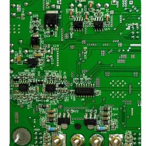
When designing PCB, it is found that many people do not understand the layers of PCB circuit board , especially the novice, the role of each layer is fuzzy. So, today we'll take a look at how the layers differ when using the software Altium Designer artboard.
1. Signal layer
The signal Layer is divided into the Top Layer (top layer) and the Bottom Layer (bottom layer). This is the layer with electrical connections, which can place components and lay out cables.
2. Mechanical layer
Mechanical is the definition of the appearance of the whole PCB board. The emphasis on "mechanical" means that it has no electrical properties, so it can be safely used to outline the shape, outline the mechanical dimensions, place the text and so on, without worrying about any change in the electrical characteristics of the board. A maximum of 16 mechanical layers can be selected.
3. Screen printing layer
Top Overlay (top screen printing layer) and Bottom Overlay (bottom screen printing layer) are used to define the top layer and bottom screen printing characters, which are some text symbols printed on the solder resistance layer, such as component name, component symbol, component pin, copyright, etc., for convenience in future circuit welding and error checking.
4. Tin paste layer
The Paste layer includes the Top Paste layer and the Bottom Paste layer, which refers to the exposed surface of the solder pad that we can see, that is, the part of the solder paste that needs to be applied before welding. Therefore, this layer is also useful in hot air leveling of the pad and making welding steel mesh.
5. Welding resistance layer
The Solder Solder layer is also often said to "open the window", including Top Solder and Bottom Solder, which is opposite to the solder paste layer, referring to the layer to cover the green oil. The layer does not stick to solder to prevent excess solder at adjacent welding points from short-circuiting during welding. The solder resistance layer covers the copper film wire to prevent the copper film from oxidizing too quickly in the air, but leaves a position at the solder joint and does not cover the solder joint.
Conventional copper coating or wiring is covered with green oil by default. If we deal with the corresponding welding resistance layer, it will prevent the green oil from covering and expose the copper.
6. Drilling layer
The Drill layers consist of Drill Gride(drill instruction Drawing) and Drill Drawing(drill drawing). The drill layers are used to provide information about the drill holes in the circuit board manufacturing process (e.g., solder pads, where holes are drilled).
7. No wiring layer
The Keep Out Layer is used to define the boundary of the wiring layer. After the keep out layer is defined, the wiring with electrical characteristics cannot exceed the boundary of the forbidden wiring layer in the future wiring process.
8. Multiple layers
The solder pad and through-hole on the circuit board need to penetrate the whole circuit board to establish electrical connection with different conductive graphic layers, so the system specially sets up an abstract layer-multilayer. Generally, the pad and the hole should be set on the multilayer, if the layer is closed, the pad and the hole can not be displayed.


Just upload Gerber files, BOM files and design files, and the KINGFORD team will provide a complete quotation within 24h.