
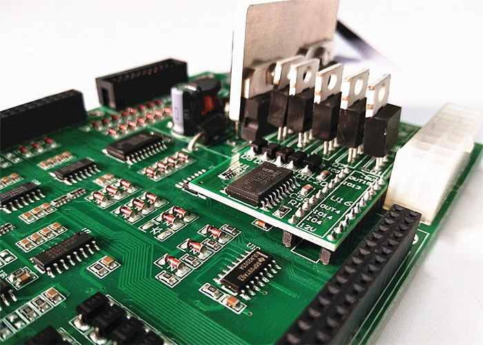
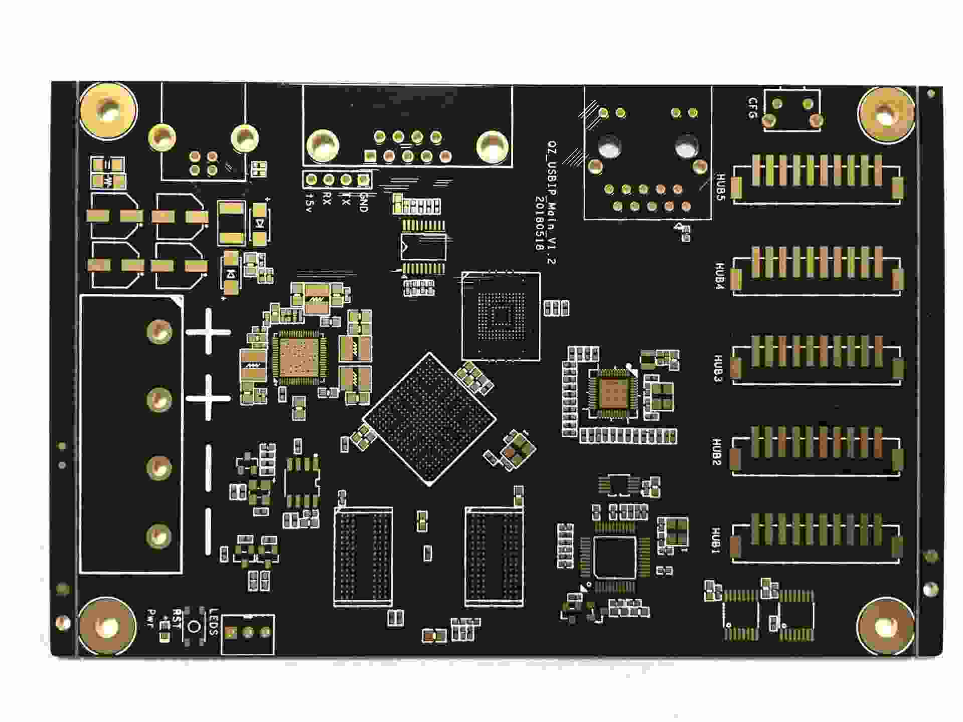
Professional PCB manufacturing and assembly
Building 6, Zone 3, Yuekang Road,Bao'an District, Shenzhen, China
+86-13410863085Mon.-Sat.08:00-20:00

This paper interprets four basic characteristics of RF circuit from four aspects: microwave RF interface, small expected signal, large disturbing signal, disturbing of adjacent channels, and gives the important elements that need special attention in PCB planning process.
Microwave RF circuits simulate small desired signals
It is necessary for the receiver to be very active in detecting small input signals. Generally, the input power of the receiver can be as small as 1 μV. The activity of the receiver is constrained by the noise emitted by its input circuit. Therefore, noise is an important factor to consider in PCB circuit board receiver planning. Moreover, the ability to guess noise with simulation tools is essential.
The noise efficiency of a front-end circuit depends primarily on the LNA, mixer, and LO. Although LNA noise can be found using traditional SPICE noise profiling, it is useless for mixers and LO, as the noise in these blocks is heavily influenced by the large LO signal.
The small input signal requires the receiver to have a great expansion function, generally requires 120 dB gain as high as. At these high gains, any signal that is coupled from the output back to the input may cause problems. An important reason for using the superheterodyne receiver architecture is that it can distribute the gain over several frequencies to reduce the probability of coupling. This also makes the frequency of the first LO different from that of the input signal, preventing the large nuisance signal from "contaminating" the small input signal.
For different reasons, the direct convers ion or homodyne architecture may replace the superheterodyne architecture in some wireless communication systems. In this architecture, the RF input signal is converted directly to the base frequency in a single process, so that most of the gain is in the base frequency, and LO is the same frequency as the input signal.
In this situation, it is necessary to understand the influence of a few couplings, and it is necessary to establish a specific model of "stray signal path", such as coupling through the substrate, coupling between the substrate and bondwire, coupling through the power line.
Rf interface for microwave RF circuit board simulation.
In concept, wireless transmitter and receiver can be divided into two parts: fundamental frequency and radio frequency. The fundamental frequency includes the frequency scale of the input signal of the transmitter and the frequency scale of the output signal of the receiver. The bandwidth of the fundamental frequency determines the fundamental rate at which data can flow through the system. The base frequency is used to improve the reliability of the data stream and reduce the load imposed by the transmitter on the transmi ssion medium under a specific data transmission rate.
Therefore, PCB planning baseband circuit, the need for a lot of signal processing engineering common sense. The RF circuit of the transmitter can convert the processed fundamental frequency signal to the specified channel, and inject the signal into the transmission media. In contrast, the receiver's RF circuit can take the signal from the transmitted medium and convert and reduce the frequency to the fundamental frequency.
Transmitters have two primary PCB planning policies:
They need to emit as much power as possible while using the least amount of power.
They should not disturb the normal operation of transceivers in adjacent channels.
As far as receivers are concerned, there are three primary PCB planning policies: First, they are necessary to accurately restore small signals; Second, they need to be able to remove disturbing signals beyond the desired channel; Finally, as with transmitters, they need to consume very little power.
Rf circuits simulate large nuisance signals
The receiver needs to be responsive to small signals, even when large disturbing signals (blockers) are present. This situation occurs when the test receives a small or distant transmission signal that is broadcast on an adjacent channel by a strong transmitter. Disturbing signals may be 60 ~ 70 dB larger than waiting signals, and can be in the input phase of the receiver in many ways to cover up, or make the receiver in the input phase of excessive noise, to block the reception of normal signals. Both of these problems occur if the receiver, during the input phase, is instigated by the nuisance source to enter the non-linear region. To prevent these problems, it is necessary that the front end of the receiver be very linear.
Therefore, "linearity" is also an important consideration when PCB board planning receiver. Since the receiver is a narrow-frequency circuit, the non-linearity is calculated by measuring "inte rmodulati on distorTI on". This involves using sine or cosine waves of two frequencies adjacent to each other in the central band (in band) to drive the input signal and then measuring the product of their reciprocal modulation. In general, SPI CE is a time-consuming and costly simulation software, because it has to perform many loops to get the desired frequency resolution to understand the distortion.
Microwave RF circuit simulation of adjacent channel annoyance
If the bandwidth is added too much, the transmitter will not be able to match the power requirements of its adjacent channels. When transmitting digitally modulated signals, it is virtually impossible to use SPICE to guess the re-growth of the spectrum. Because the transfer operations of approximately 1000 digital symbols need to be simulated to obtain representative spectrum, combined with high frequency carriers, these make transient profiling of SPICE impractical.
Distortion also plays an important role in the transmitter. The nonlinearity of the transmitter in the output circuit may cause the bandwidth of the transmitted signal to be distributed in adjacent channels. This phenomenon is called spectral regrowth. Before the signal reaches the power expander (PA) of the transmitter, its bandwidth is constrained; But "cross-modulation distortion" in PA causes the bandwidth to be added again.
PCB related concepts
Feb 14,2023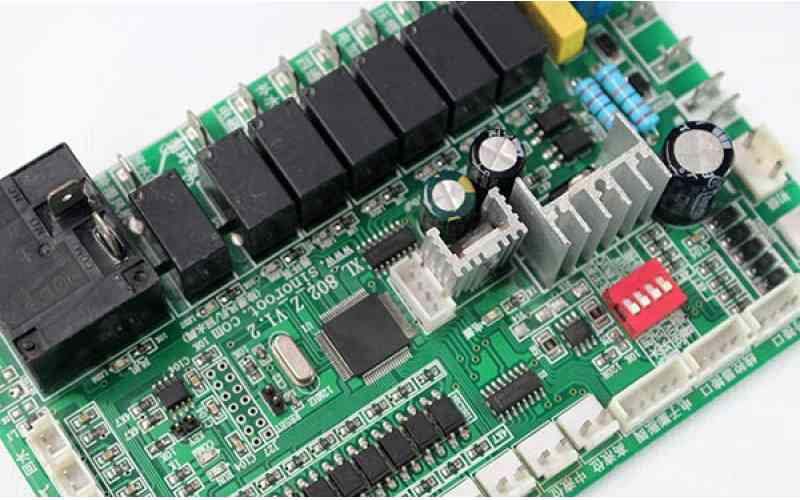


Just upload Gerber files, BOM files and design files, and the KINGFORD team will provide a complete quotation within 24h.