
Professional PCB manufacturing and assembly
Building 6, Zone 3, Yuekang Road,Bao'an District, Shenzhen, China
+86-13410863085Mon.-Sat.08:00-20:00

HDI circuit board (High Density Interconnector), namely high density interconnector, is a circuit board with high density of line distribution using micro-blind buried hole technology. HDI board has an inner line and an outer line, using drilling, hole metallization and other processes, so that each layer of lines inside the successful connection.
HDI circuit board is generally considered appropriate and the use of stacking method, the more the stacking number, the higher the technical grade of the board. The ordinary HDI board is basically 1 layering, the high level HDI circuit board is considered appropriate and the use of 2 or more layering technology, at the same time is considered appropriate and the use of advanced PCB technology such as stacking holes, electroplating holes, laser direct drilling.
When the density of PCB increases to more than eight layers of board, HDI circuit board is used to produce, its cost will be more complex than the traditional pressing process to groove. HDI boards are helpful in the application of advanced construction technology, with higher electrical performance and signal accuracy than traditional PCBS. In addition, HDI board has better improvement for radio frequency interference, electromagnetic wave interference, electrostatic release, thermal conductivity and so on.
Electronic products continue to high density, high precision progress, the said "high", in addition to the growth of machine performance, but also by the size of the small machine. High density integration (HDI) technology enables end-product presets to be smaller, while satisfying higher standards of electronic performance and speed. Until now, many popular electronic products, such as mobile phones, digital cameras, laptops, transportation electronics, etc., are using HDI boards. With the upgrading of electronic products and the needs of the market, the progress of HDI board will be very fast.
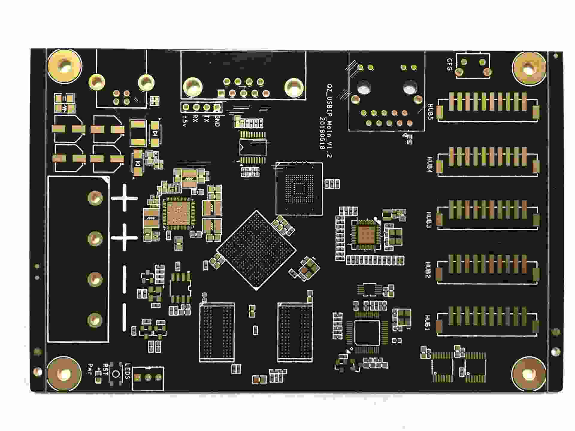
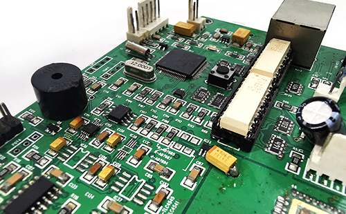
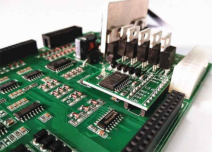
Ordinary PCB circuit board Shao Jie
PCB (Printed Circuit Board), Chinese name for printed circuit board, also known as printed circuit board, is a closed electronic device, is the support body of the electronic component, is the electrical component of the carrier. Because it is made using electronic printing as it sees fit, it is called a "printed" circuit board.
Its utility is mainly electronic facilities think appropriate and use of printed board, because of the same kind of printed board, so prevent the error of manual wiring, and can successfully achieve electronic components semi-automatic insertion or paste, semi-automatic soldering, semi-automatic inspection and determination, to ensure the quality of electronic facilities, increase the labor production rate, reduce the cost, and easy maintenance.
HDI board is high density interconnected circuit board, blind hole electroplating and second pressing board are HDI board, divided into first order, second order, third order, fourth order, fifth order HDI board, such as the iPhone 6 motherboard is the fifth order HDI board.
Innocent burials are not necessarily HDI boards.
HDI PCB first order and second order and third order how to distinguish
The first order is relatively simple, the process and technology are good choke.
Second order is the problem, one is the counterpoint problem, one is the punching and copper plating problem. There are a variety of second-order presuppositions. One is that each stage gives way to each other. When the secondary adjacent layer is required to be jointly signed, it is connected through the wire at the mid-waist layer, which is equivalent to two first-order HDI.
In the second case, two first-order holes are stacked on top of each other, and the second order is successfully achieved in a superimposed form. The processing is also roughly similar to that of the two first-order holes, but there are a number of process elements that must be particularly restrained, which is mentioned above.
The third is directly from the outer layer to the third layer (or N-2 layer), the process and in front of many different, the degree of difficulty is greater.
For the third order, the second order analogy is.
The usual PCB board material is FR-4, which is a natural epoxy resin and electronic grade glass cloth pressed together. Ordinary traditional HDI circuit board, the most outside to use adhesive copper foil, because laser drilling, there is no way to get through the glass cloth, so the ordinary use of non-glass fiber adhesive copper foil, but today's high energy laser drilling machine has been able to play through 1180 glass cloth. So there's no difference from the usual material.


Just upload Gerber files, BOM files and design files, and the KINGFORD team will provide a complete quotation within 24h.