
Professional PCB manufacturing and assembly
Building 6, Zone 3, Yuekang Road,Bao'an District, Shenzhen, China
+86-13410863085Mon.-Sat.08:00-20:00

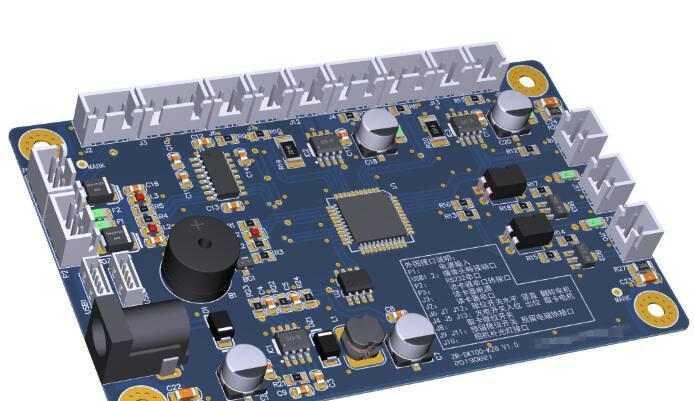
One, PCB circuit board introduction
PCB circuit board (printed circuit board), with insulation board as the base material, cut into a certain size, it is attached with at least one conductive graphic, and distributed with holes (such as component holes, fastening holes, metallization holes, etc.), used to replace the chassis of the previous device electronic components, and realize the mutual connection between electronic components. Because this board is made by electronic printing, it is called "printed circuit board".
Two, the basic composition of PCB circuit board
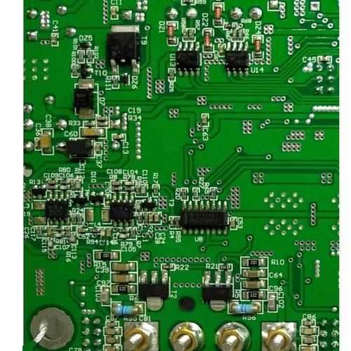
The current circuit board is mainly composed of:
1. Circuit and Pattern: Circuit is used as a tool for conduction between originals. In the design, large copper surface will be designed as the grounding and power layer. The lines and drawings are made at the same time.
Dielectric Layer: They will be used to maintain insulation between the line and each layer also known as the substrate.
3, Through hole/via: through hole can make the lines of two levels and above through each other, the larger through hole is used as part plug-in, in addition, the non-through hole (nPTH) is usually used as surface mounting positioning, assembly for fixing screws.
4. Solder resistant ink (Solder resistant /Solder Mask) : Not all the copper surface needs to eat the parts on the tin. Therefore, a layer of material (usually epoxy resin) that prevents the copper surface from eating the tin will be printed in the non-solder area to avoid short circuit between the non-solder lines. According to different processes, divided into green oil, red oil, blue oil.
5, Legend /Marking/Silk screen: this is not necessary, and its main function is to mark the name and position frame of each part on the circuit board for convenient maintenance and identification after assembly.
6. Surface Finish: Because the copper surface is easily oxidized in the general environment, it cannot be tinned (poor soldering), so it will protect the copper surface to eat tin. Protection methods include Tin spray (HASL), gold (ENIG), Silver (Immersion Silver), tin (Immersion tin), organic flux protection (OSP), each method has advantages and disadvantages, collectively known as surface treatment.
Three, the importance of PCB circuit boards
It is an important electronic component, is the support body of electronic components.
Printed circuit boards are not common terminal products, and the definition of the name is somewhat confusing.
For example: personal computer with the mother board, called the motherboard, but not directly called the circuit board, although there is a circuit board in the host board, but not the same, so the evaluation of the industry is related to the two can not say the same.
Another example: because there are integrated circuit parts on the circuit board, so the news media called it IC board, but it is not the same as printed circuit board. What we usually refer to as a printed circuit board is a bare board -- a circuit board with no components on it.
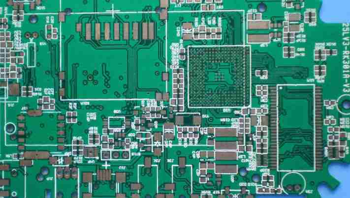
Four, PCB circuit board classification
According to the PCB printed circuit board layer classification: PCB printed circuit boards are divided into single panel, double panel and multi-layer board. The common multilayer board is generally 4 layers or 6 layers, complex multilayer board can reach dozens of layers.
There are three main types of PCB boards:
1. Single-sided circuit board
Single-side boards On the most basic PCB, the parts are concentrated on one side and the wires on the other. Because wires appear on only one side, this type of PCB is called Single-sided. Only early circuits used such boards because a single panel had many severe limitations on the design circuit (because there was only one side, the wiring could not be crossed and had to be routed in a separate path).
2. Double-sided circuit board
Double-sideboards are wired on both sides of a circuit board, but to use the wires on both sides, proper circuit connections must be made between the two sides. This "bridge" between circuits is called a pilot hole (via). A pilot hole is a small hole on a PCB filled with or coated with metal that can be connected to the wires on both sides. Because the area of the dual panel is twice as large as that of the single panel, the dual panel solves the difficulty of the single panel due to the interleaving of the wiring (it can be routed to the other side through the hole), and it is more suitable for the more complex circuit than the single panel.
3, multilayer circuit board
To increase the area that can be wired, Multi-LayerBoards use more single or double-sided wiring boards. With a double-sided for the inner layer, two single-sided for the outer layer, or two double-sided for the inner layer, two single-sided for the outer layer of the printed circuit board, through the positioning system and insulating binder material alternating together and conductive graphics in accordance with the design requirements of the printed circuit board is a four-layer, six-layer printed circuit board, also known as the multilayer printed circuit board.
The number of layers of the board does not mean that there are several independent wiring layers. In special cases, empty layers will be added to control the thickness of the board. Usually, the number of layers is even and includes the outermost two layers. Most of the main board is a 4 - to 8-layer structure, but the technology can theoretically do close to 100 layers of PCB board. Most large supercomputers use quite a few layers of mainframe boards, but because such machines can be replaced by clusters of ordinary computers, super-multiboards have fallen out of use. Because the layers in the PCB are so tightly integrated, it is not always easy to see the actual number, but if you look closely at the main board, you can see it.


Just upload Gerber files, BOM files and design files, and the KINGFORD team will provide a complete quotation within 24h.