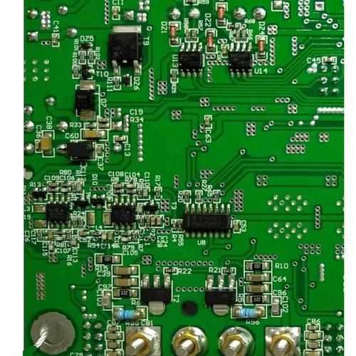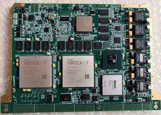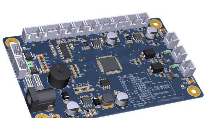
Before the advent of the printed circuit board, the interconnection of electronic components relied on wires directly connected to form a complete circuit. Today, circuit breadboards exist only as effective experimental tools, while printed circuit boards have become the dominant position in the electronics industry.
At the beginning of the 20th century, in order to simplify the production of electronic machines, reduce wiring between electronic parts and reduce production costs, people began to study the way to replace wiring by printing. For thirty years, engineers have proposed adding metal conductors to the insulated substrate as wiring.
The most successful was in 1925, when Charles Ducas of the United States printed circuit patterns on insulated substrate, and then successfully built conductors for wiring by electroplating.
It wasn't until 1936 that Paul Eisler, an Austrian, introduced foil film technology in Britain, using printed circuit boards inside a radio set. In Japan, palace this pleased help to spray the attached wiring method "メ タ リ コ ン blowing wiring method (chartered 119384)" success to apply for a patent. Of the two, Paul Eisler's method, which is most similar to today's printed circuit boards, is called subtracting, in which unwanted metal is removed. Charles Ducas and Kinosuke Miyamoto did this by adding only the wiring needed, called the addition method. However, because of the high heat of the electronic parts at that time, the substrate of the two was difficult to use together, so there was no formal use, but also made the printed circuit technology further.

In 1941, the United States painted copper paste on talc for wiring, to make contact fuse.
In 1943, the Americans used the technology in large numbers in military radios.
In 1947, epoxy resins began to be used for manufacturing substrates. At the same time, NBS began to develop printed circuit technology to form coils, capacitors, resistors and other manufacturing technologies.
In 1948, the United States officially approved the invention for commercial use.
It was not until the 1950s, when transistors with lower calorific value largely replaced vacuum tubes, that printed circuit plates became widely adopted. At that time, etched foil film technology was the mainstream.
In 1950, Japan used a glass substrate with silver paint as wiring; And paper phenolic substrate (CCL) made of phenolic resin with copper foil as wiring.
In 1951, the appearance of polyimide, the resin further heat resistance, also made polyimide substrate.
In 1953, Motorola developed the electroplating through hole method of dual panel. This method is also applied to the later multilayer circuit board.
In the 1960s, 10 years after printed circuit boards were widely used, their technology was becoming more mature. Since Motorola's dual panels were introduced, multiple layers of printed circuit boards have appeared, increasing the wiring to substrate area ratio.
In 1960, V. Dahlgreen created a flexible printed circuit board with a metal foil film printed with a circuit attached to a thermoplastic.
In 1961, the Hazeltine Corporation in the United States produced multilayer board based on the electroplating through hole method.
In 1967, Plated-up technology, one of the ways to add layers, was published.
In 1969, FD-R made soft printed circuit boards with polyimides.
In 1979, Pactel announced the Pactel Method, one of the additional layer methods.
In 1984, NTT developed the "Copper Polyimide process" for thin-film circuits.
In 1988, Siemens developed the Microwiring Substrate for additional layer printed circuit boards.
In 1990, IBM developed "Surface Laminar Circuit" (SLC) added layer printed circuit boards.
In 1995, Matsushita developed ALIVH's layered printed circuit board.
In 1996, Toshiba developed Bit's additive printed circuit board.
At the end of the 1990s, when many additional PCB board schemes were proposed, the additional PCB was also formally put into practice in large quantities until now.


