
Professional PCB manufacturing and assembly
Building 6, Zone 3, Yuekang Road,Bao'an District, Shenzhen, China
+86-13410863085Mon.-Sat.08:00-20:00

Abstract: PCB research and development began in 1956, 1963 to 1978 gradually expanded to form PCB industry. In 2002, it became the third largest PCB manufacturer. In recent years, the PCB industry in our country has maintained the high growth of about 20%, which is much higher than the growth of the global PCB industry. Since 2005, the world's electronic circuit industry technology has developed rapidly, mainly focusing on passive component PCB, inkjet PCB process, laser direct imaging technology, optical technology PCB and nanomaterials in PCB board applications.
1 Printed circuit board industry and technical development
1.1 Definition of printed circuit boards
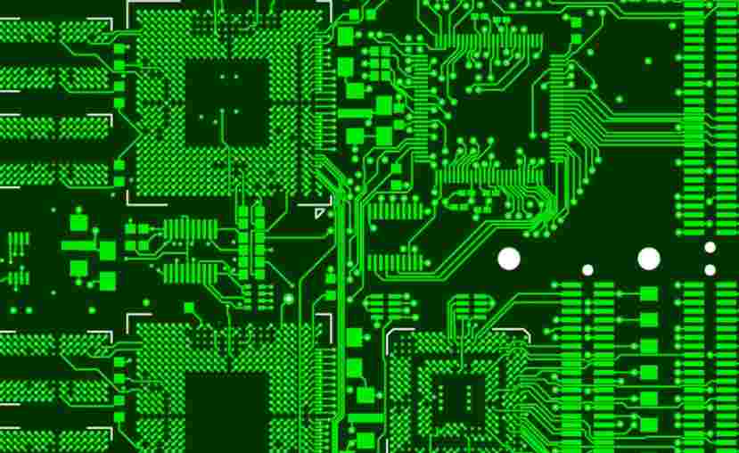
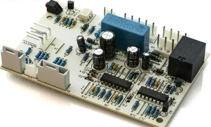
Printed circuit board, also known as printed circuit board, printed circuit board, short for printed circuit board, English abbreviation PCB (printed circuit board) or PWB (printed circuit board), it is based on the insulation board, cut into a certain size, affixed to it at least one conductive pattern, And layout holes (such as component holes, fastening holes, metallization holes, etc.) to replace the past electronic components of the chassis installation, interconnection between the electronic components. Because such boards are made using electronic printing technology, they are called "printed" boards. The printed circuit board is the key interconnection of electronic equipment, and plays an important supporting role in the major breakthroughs in scientific research, communication, automotive, aerospace and other fields. It is the important foundation of modern science and technology. The continuous improvement of its own development and related technologies has promoted the continuous development of social economy.
1.2 The PCB industry development in our country
The research and development of PCB in China began in 1956, and the PCB industry expanded gradually from 1963 to 1978. After more than 20 years of reform and opening up, due to the introduction of foreign advanced technology and equipment, single-sided, double-sided and multi-layer board has achieved rapid development, and the domestic PCB industry has gradually developed from small to large. In 2002, it became the third largest PCB manufacturer. In 2003, the output value, import and export value of PCB exceeded $6 billion, surpassing the United States for the first time and becoming the second largest PCB producing country in the world. The share of output value also doubled from 8.54% in 2000 to 15.30%. In 2006, China replaced Japan as the world's largest PCB production base and the most active country in technological development. In recent years, the PCB industry in our country has maintained the high growth of about 20%, which is much higher than the growth of the global PCB industry. On March 17, 2008, China printed circuit Industry Association established Full Print electronic branch in Shanghai, indicating that our PCB industry development to a new level.
1.3 PCB technology development in our country
Since 2005, the world's electronic circuit industry technology has developed rapidly, focusing on passive component PCB, inkjet PCB technology, laser direct imaging technology, optical technology PCB, nanomaterials in PCB applications. PCB from the installation to the sealing board development, as well as components of the chip and integration, ball grid array, chip level packaging, multi-chip module more and more popular. PCB packaging terminals are required to be refined and highly integrated. At the same time, the substrate is required to assume new functions. Printed boards with embedded components appear to meet the requirements of high-density assembly.

At present, advanced PCB manufacturing technologies include: high density inner layer (HDI) printed board manufacturing process, semi-addition technology, thermosetting ink layering (TCD) technology, electroplating blind hole filling technology, high grade special material printed board manufacturing technology, etc.
2 Chinese PCB patent analysis
In the database of the State Intellectual Property Office, the topic search is mainly conducted from the technical point of view of PCB production. The total number of patent applications from 1985 to 2010 was 2,385, and that from 2000 to 2010 was 2,108, accounting for 88% of the total number of patent applications in the last ten years. From 2000 to 2010, it applied for 1,798 invention patents and 310 utility models; We have applied for 1,677 national patents and 431 international patents. From the patent number, it shows that PCB industry has developed rapidly in recent ten years.
Foreign countries have applied for patents in our country: Japan, the United States, Korea, Germany, France, Finland, Sweden, the Netherlands, Singapore, etc. It can be seen that many foreign companies have applied for patents in China, indicating that the Chinese market is increasingly influenced by foreign companies. Notice, there's more competition. Top 10 cities with patent applications: Guangdong, Taiwan, Jiangsu, Shanghai, Zhejiang, Beijing, Fujian, Shandong, Hubei, Tianjin. Chinese patent applications are mainly distributed in the Pearl River Delta and the Yangtze River Delta along the southeast coast. The Yangtze River Delta, which accounts for more than 90 percent of the country, has developed rapidly in recent years, while the northeast has developed relatively slowly.
3 PCB product structure analysis in our country
From the perspective of PCB layer number and development direction, PCB industry is divided into single side, double side, conventional multilayer board, flexible board, HDI (high density interconnect) board, packaging substrate and other six product segments. From the perspective of the four cycles of product life cycle "introduction period - maturity period - decline period", single and double panel is in the decline period because it does not adapt to the short, light and thin application trend of current electronic products, and the proportion of its output value gradually declines. Japan, South Korea, Taiwan and other developed countries and regions rarely produce such products locally, and many large factories have made it clear that they will no longer accept orders for double-sided panels.
What does impedance mean to PCB boards?
Feb 10,2023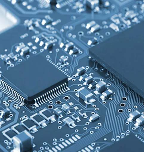


Just upload Gerber files, BOM files and design files, and the KINGFORD team will provide a complete quotation within 24h.