
Professional PCB manufacturing and assembly
Building 6, Zone 3, Yuekang Road,Bao'an District, Shenzhen, China
+86-13410863085Mon.-Sat.08:00-20:00

PCB multilayer board introduction:
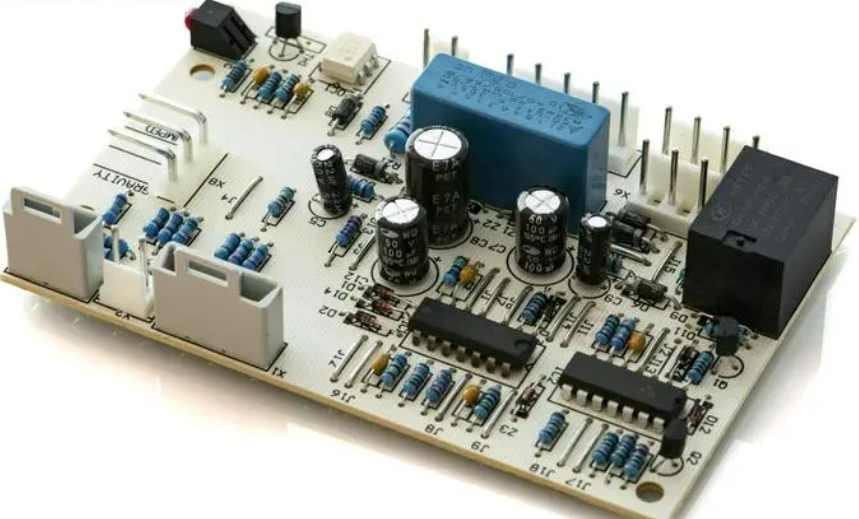
PCB double panel is a mid-middle layer of media, both sides are line layer. PCB multilayer board is the multi-layer line layer, between each two layers is the media layer, the media layer can do very thin. A multilayer circuit board has at least three conductive layers, two of which are on the outside, and the remaining layer is synthesized into an insulating board. The electrical connection between them is generally achieved by plating through holes on the cross section of the current flow plate.
PCB multilayer board origin:
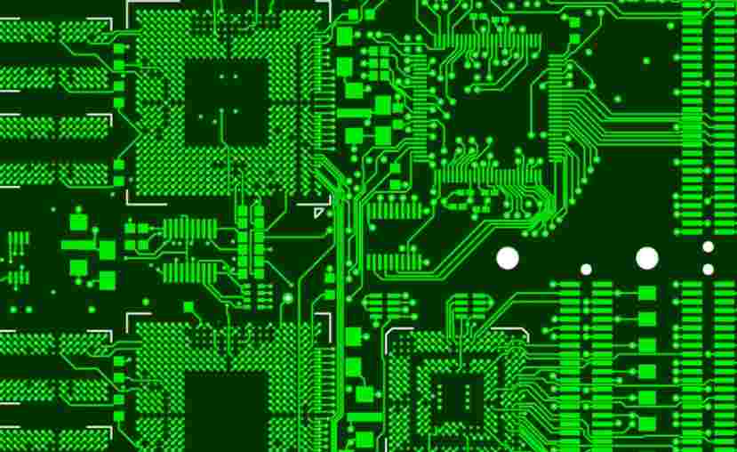
Because of the increase in the density of integrated circuit packaging, resulting in a high concentration of lines, the use of this much substrate becomes necessary. In the layout of printed circuit, unforeseeable preset problems, such as noise, stray capacitance, crosstalk, etc., appear. Therefore, the printed circuit board presets must focus on minimizing the length of signal lines and preventing parallel routes. Obviously, none of these needs can be satisfied in a single panel, or even in a dual panel, because of the limited number of interleavings that can be successfully implemented. In the case of a number of interconnection and interleaving needs, the circuit board to achieve a satisfied performance, it is necessary to expand the board layer to more than two layers, so the multilayer circuit board is exposed. Because the original aspiration of the multilayer circuit board was to provide more freedom to select the appropriate routing routes for complex and/or noise-sensitive electronic circuits. A multilayer circuit board has at least three conductive layers, two of which are on the outside, and the remaining layer is synthesized into an insulating board. The electrical connection between them is generally achieved by plating through holes on the cross section of the current flow plate. Errors are not explained otherwise. The multilayer printed circuit board is the same as the double panel, which is usually plated through hole plate.
PCB multilayer board explanation:
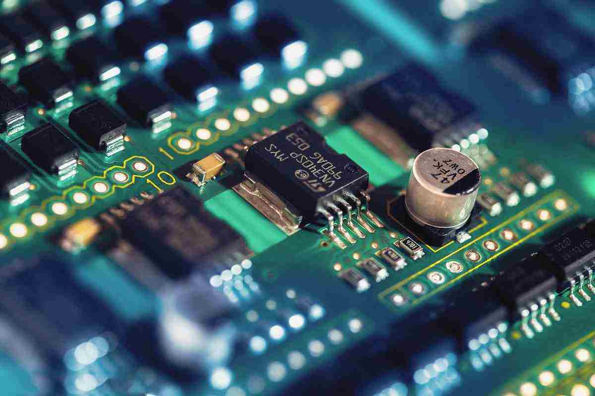
PCB multilayers are made by stacking two or more layers of circuits on top of each other, with a reliable pre-set interconnection between them.Because the layers are drilled and electroplated before they are all rolled together, the technique goes against the conventional manufacturing process. The inner two layers are made up of traditional double panels, while the outer layers are made up of separate single panels. Prior to rolling, the inner substrate will be drilled, electroplated through holes, pattern transfer, development, and die etching. The outer layer to be drilled is the signal layer, which is plated in the form of a ring of balanced copper at the inner edge of the through hole. Then each layer is rolled together to form a multi-substrate, which can be used to implement the wave welding (between components) mutual sign-on.Crushing may be done in a hydraulic press or in an overpressure chamber (autoclave). In a hydraulic press, the prepared material (for pressure stacking) is placed under cold or preheated pressure (materials with high glass change temperature are placed in a temperature of 170-180 ℃). The glass transition temperature is the range of amorphous regions of amorphous polymers (natural resins) or locally crystalline polymers from a firm, hard, fairly brittle state to a viscous, rubbery state.
PCB multi-layer board application:
Multilayer panels are used in professional electronic equipment (computers, military installations), especially in the case of weight and size over load. But this is only a trade-off between the increased cost of multiple substrates and the increased space and reduced weight. Multisubstrate is also useful in high speed circuits. They can provide the presetters of printed circuit boards with more than two layers of board to lay wires, and provide a large area of ground and power supply.


Just upload Gerber files, BOM files and design files, and the KINGFORD team will provide a complete quotation within 24h.