
Professional PCB manufacturing and assembly
Building 6, Zone 3, Yuekang Road,Bao'an District, Shenzhen, China
+86-13410863085Mon.-Sat.08:00-20:00

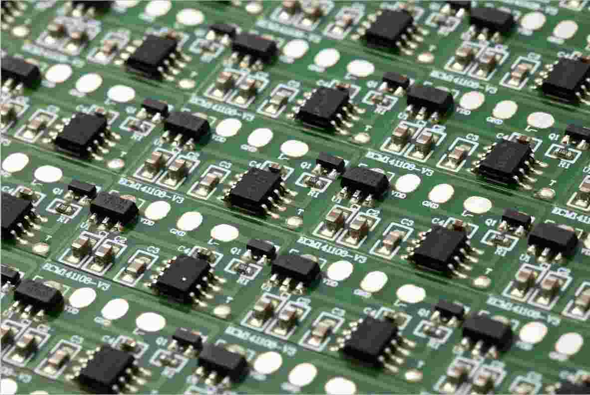
In electronic products and equipment, the circuit board is an indispensable component, it plays the electrical and mechanical connection of the circuit system. It is one of the main tasks of PCB designer how to arrange and combine the circuit components on PCB according to certain requirements.
Layout design is not as simple as arranging components on a PCB or connecting circuits. Practice has proved that a good circuit design must have a reasonable component layout, so that the circuit system can achieve stable and reliable work after entity combination. On the contrary, if the component layout is not reasonable, it will affect the performance of the circuit board, and even can not work.
Matters needing attention for component packaging in RF circuit
Successful RF design requires careful attention to every step and detail of the entire design process, which means thorough and careful planning at the beginning of the design phase, as well as comprehensive and continuous evaluation of the progress of each design step. And this kind of meticulous design skills is the lack of most domestic electronic enterprise culture.
In recent years, the demand and growth of Bluetooth devices, wireless Local area network (WLAN) devices, and mobile phones has led to a growing focus on RF circuit design techniques. RF circuit board design, like electromagnetic interference (EMI) problems, was and still is the most difficult part of engineers to control, even a nightmare. If a design is to be successful in one go, it requires careful planning and attention to detail.
Radio frequency circuit board design is often described as a kind of "black art" because of the theoretical uncertainties. But this is only a partial to cover the whole point of view, RF circuit board design or there are many rules to follow. However, when it comes to actual design, the really useful trick is how to compromise these rules when they cannot be implemented due to various constraints. Important RF design topics include: impedance and impedance matching, insulating material and laminates, wavelengths and harmonics Etc.
In the course of WiFi product development, RF circuit wiring is a very key process. Most of the time, we may have been designed in principle is very perfect, but in the actual board, after the piece found is not ideal, in fact, these are the wiring is not perfect. This article will be a wireless card wiring example and my little work experience for you to explain the RF circuit in the wiring should pay attention to some problems.
The stacking of circuit boards
Before wiring, we must first determine the layout of the circuit board, just like building a house to have the walls of the house. The determination of the circuit board structure is related to the complexity of the circuit design, electromagnetic compatibility considerations and many other factors.
In the PCB board stacking of wireless network card, the situation of single panel will not appear basically, so this paper will not discuss the situation of single panel. The problems that should be paid attention to in the design of two layer board.
In the design of four-layer board, we generally use the second layer as the complete ground plane, and at the same time, we will also put important signal lines on the top layer (including radio frequency lines of course), in order to better control the impedance. In a design of six or more layers, we would also use the second floor as a complete floor plan, and then run the most important signal line on the top floor.
Impedance control
After we carried out the principle design and simulation, one thing worth noting in Layout is impedance control. As we all know, we should try to ensure that the characteristic of the Line is 50 ohms, which is mainly related to the line width, in this case, two and a half layers. The Surface Coplanar Line model is used to calculate the impedance in Polar.
Placement of RF components
I believe that those who have done RF design should know that we should try our best to make the length of the wiring shorter, and the more compact the placement of the components (except for special requirements). At the same time, we should try our best to ensure that the placement of the components is favorable to the wiring (do not make the wiring go around).
Precautions for RF cabling
As mentioned above, the length of RF cable should be as short as possible, and the line width should be set in strict accordance with the calculated value. It is especially important to pay attention to that there is no sharp break point in the RF routing, and it is best to use an arc at the turning point of the routing.
Second, in multilayer board wiring, it is possible that the important RF lines will inevitably cross, and then we need to use the last thing we want to use: through holes. In this way, some RF signal lines will go to the bottom layer or even the middle layer. However, no matter which layer, there must be a reference plane for RF cable routing. At this time, a noteworthy problem is not to cross layers or make the ground plane discontinuous.
Through hole placement
The hole placement is really a more complicated thing, this article only discusses the kind of grounded hole.
First of all, the ground wire next to the RF cable had better be perforated through the hole and connected to the ground plane of the bottom or middle layer, so that any interference signal or radiation can have the shortest path to the ground. However, the distance between the hole and the RF signal line should not be too close, otherwise the RF signal quality will be seriously affected, which can be flexibly controlled in the actual design process.
Secondly, in the large area of the ground plane, we usually place a lot of holes to connect different layers of the ground. This in the wiring of the radio frequency circuit, it should be noted that the big hole should not be played regularly, it is best to make a diamond shape, so as to maximize the suppression of all kinds of interference.

Patch processing which good how to choose
Feb 06,2023


Just upload Gerber files, BOM files and design files, and the KINGFORD team will provide a complete quotation within 24h.