
Professional PCB manufacturing and assembly
Building 6, Zone 3, Yuekang Road,Bao'an District, Shenzhen, China
+86-13410863085Mon.-Sat.08:00-20:00

When processing and testing high frequency PCB board and high frequency antenna, there are often beginners, because the selection of incorrect high frequency PCB leads to unsatisfactory product results. Today, let's talk briefly. What are the PCB high frequency plates? How to choose? Definition of PCB high frequency board
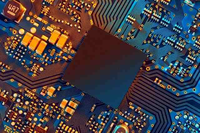
High frequency circuit board refers to the special circuit board with high electromagnetic frequency, which is used for PCB in the field of high frequency (frequency greater than 300MHZ or wavelength less than 1 meter) and microwave (frequency greater than 3GHZ or wavelength less than 0.1 meter). It is a circuit board which is produced by using part of the manufacturing process of the common rigid circuit board or by using a special processing method on the microwave-based copper clad board. Generally speaking, high-frequency boards can be defined as circuit boards with frequencies above 1GHz.
With the rapid development of science and technology, more and more equipment are designed in microwave frequency band. 1GHZ) even with the field of millimeter wave (77GHZ) above the application (such as now very popular vehicle 77GHz millimeter wave antenna), which also means that the frequency is higher and higher, the requirements of the circuit board substrate is also higher and higher. For example, the substrate material needs to have excellent electrical properties, good chemical stability, with the increase of power signal frequency on the substrate loss requirements are very small, so the importance of high frequency plate is highlighted.
Classification of PCB high frequency circuit boards
1. By material:
(1) Organic material: phenolic resin, glass fiber/epoxy resin, etc.
(2) Inorganic material: aluminum, Copper-invar-copper, ceramic, etc. Mainly for its heat dissipation function
2, according to the product soft and hard
(1) Rigid board , (2) Flexible PCB, (3) Rigid-Flex PCB
3, according to the structure
(1) single panel, (2) double panel, (3) multilayer board
4, according to the use of points
Communications/consumable electronics/military/computer/semiconductor/electrical test board...
Choose high frequency high speed PCB material what are the important indicators
When selecting the substrate used for PCB of high frequency circuit, special investigation should be made on the variation characteristics of the material DK at different frequencies. And for the requirements that focus on high-speed signal transmission, or characteristic impedance control requirements, focus on DF and its performance under the conditions of frequency, temperature and humidity.
Under the condition of frequency change, the DK and DF values of general substrate materials show a great change rule. Especially in the frequency from l MHz to l GHz, the change of DK and DF values is more obvious. For example, the DK value of the generic epoxy-glass cloth based substrate material (generic FR-4) is 4.7 at lMHz and the DK value varies 4.19 at lGHz. When the DK value exceeds lGHz, the change trend is gentle. Its change trend is to decrease with the increase of frequency (but the range of change is small), for example, in l0GHz, the DK value of general FR 1 4 is 4.15, with high speed, high frequency characteristics of substrate materials in the case of frequency change, DK value change is small, from lMHz to lGHz change frequency, DK is kept in the range of 0.02. The DK value has a slight tendency to decrease under different frequency conditions from low to high.

The dielectric loss factor (DF) of the general substrate material, under the influence of the frequency change (especially in the high frequency range), the DF value changes more than DK. Therefore, when evaluating the high frequency characteristics of a substrate material, the key point to be investigated is the change of its DF value. For substrate materials with high speed and high frequency characteristics, there are two distinct types of general substrate materials in terms of changing characteristics under high frequency. One is that with the change of frequency, its (DF) value changes very little. Another class is similar to the general substrate material in the range of change, but its own (DF) value is low.
How to choose high frequency circuit board high speed plate
PCB board selection must meet the design requirements, mass production, cost balance. In short, the design requirements include both electrical and structural reliability. This board issue is often important when designing very high speed PCB boards (frequencies greater than GHz). For example, now commonly used FR-4 material, at a few GHz frequency Df dielectric loss (Dielectricloss) will be large, may not be suitable.
For example, a 10Gb/S high-speed digital signal is a square wave, which can be viewed as a superposition of sine-wave signals of different frequencies. Therefore, 10Gb/S contains many different frequency signals: 5Ghz fundamental signal, 3th-order 15GHz, 5th-order 25GHz, 7th-order 35GHz signal and so on. Maintaining the integrity of the digital signal and the steepness of the upper and lower edges is similar to the low loss and low distortion of RF microwave transmission (the high frequency harmonic portion of the digital signal reaches the microwave band). Therefore, in many respects, the requirements for PCB selection for high-speed digital circuits are similar to those for RF and microwave circuits.
In the actual engineering operation, the selection of high-frequency board seems simple, but there are many factors to be considered. Through the introduction of this paper, as a PCB design engineer or a person in charge of high-speed project, I have a certain understanding of the characteristics and selection of board. Understand the electrical properties, thermal properties, reliability, etc. And the rational use of overlapping, design a piece of high reliability, good processing products, a variety of factors to consider the optimization.
The following will be introduced respectively, the selection of appropriate plate main considerations:
1. Manufacturability:
For example, how many times pressing performance, temperature performance, CAF/ heat resistance and mechanical toughness (viscosity) (good reliability), fire rating;
2. Various performance (electrical, performance stability, etc.) matching with the product:
Low loss, stable Dk/Df parameters, low dispersion, small variation coefficient with frequency and environment, small material thickness and rubber content tolerance (good impedance control), if the line is long, consider low roughness copper foil. In addition, simulation is needed in the early stage of high-speed circuit design, and the simulation result is the reference standard for design. "Xingsen Technology-Agilent (High Speed/RF) Joint Laboratory" has solved the performance problem of inconsistency between simulation results and test results, and has done a lot of closed-loop verification of simulation and actual test, which can achieve consistency between simulation and test through unique methods.
3. Timely availability of materials:
Many high-frequency plate procurement cycle is very long, even 2-3 months; In addition to the conventional high frequency plate RO4350 has inventory, many high frequency plates need to be provided by customers. Therefore, high frequency plate needs to communicate well with manufacturers in advance and prepare materials as soon as possible;
4. Cost factor
Look at the price sensitivity of the product, whether it is consumer products, or communications, medical, industrial, military applications;
5. Applicability of laws and regulations:
To integrate with different national environmental laws and regulations, to meet the requirements of RoHS and halogen free.
Among the above factors, the running speed of high-speed digital circuit is the main factor to be considered in PCB board selection. The higher the circuit speed, the smaller the selected PCB Df value should be. With medium, low loss circuit board will be suitable for 10Gb/S digital circuit; 25Gb/s digital circuit is suitable for plates with lower losses; The ultra-low loss sheet will accommodate faster, high-speed digital circuits at speeds of 50Gb/s or more.
Seen from the material Df:
Df between 0.01 and 0.005 circuit plates are suitable for digital circuits with an upper limit of 10Gb/S;
Df between 0.005 and 0.003 circuit plates are suitable for digital circuits with an upper limit of 25Gb/S;
Df no more than 0.0015 circuit board suitable for 50Gb/S or even higher speed digital circuits.
Processing method:
One. Opening: must retain the protective film opening, to prevent scratches, indentation
Two. Drilling:
1. Use new drill nozzle (standard 130), one piece in a stack is the best, press foot pressure is 40psi
2. The aluminum sheet is the cover plate, and then the PTFE plate is tightened with 1mm dense amine pad
3. Blow the dust out of the hole with an air gun after drilling
4. Use the most stable drill, drilling parameters (basically, the smaller the hole, the faster the drilling rate, the smaller the Chip load, the smaller the return rate)
Three. Hole treatment
Plasma treatment or sodium naphthalene activation treatment is conducive to through hole metallization
Four.PTH copper sinking
1. After micro-etching (controlled by the micro-etching rate of 20 microinches), pull into the plate from the deoil cylinder at PTH
2. If necessary, go through the second PTH, just from the forecast? The cylinder began to feed into the plate
Five.Welding resistance
1. Pre-treatment: acid washing plate, not mechanical grinding plate
2. After pretreatment, bake plate (90℃, 30min), brush green oil for curing
3. Divided into three sections of baking plate: one section of 80℃, 100℃, 150℃, 30min each (if there is oil dumping on the substrate surface, you can rework: wash off the green oil, reactivate the treatment)
Six. Gong board
Lay the white paper on the PTFE board line surface and clamp it with a 1.0MM thickness of etched coppered FR-4 substrate or phenolic substrate


Just upload Gerber files, BOM files and design files, and the KINGFORD team will provide a complete quotation within 24h.