
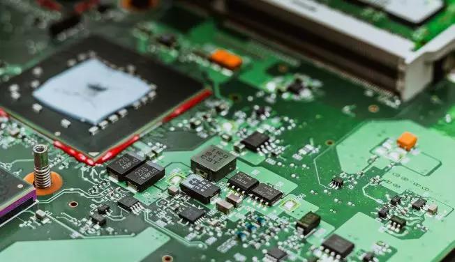
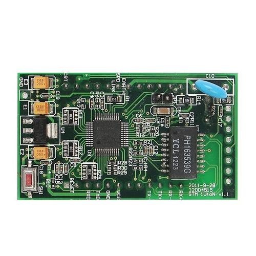
Professional PCB manufacturing and assembly
Building 6, Zone 3, Yuekang Road,Bao'an District, Shenzhen, China
+86-13410863085Mon.-Sat.08:00-20:00

Flexible circuit board is made of polyimide or polyester film as a substrate with high reliability, excellent flexibility of the printed circuit board. Soft board or FPC for short. It has the characteristics of high wiring density, light weight and thin thickness. It is mainly used in many products such as mobile phones, laptops, PDAs, digital cameras, and LCM.
Types of FPC
Single-layer FPC
Having a chemically etched conductive pattern layer, the conductive pattern layer on the flexible insulating substrate surface is calendered copper foil. The insulating substrate may be polyimide, polyethylene terephthalate, arylamide fiber ester and polyvinyl chloride. Single-layer FPC can be divided into the following four subcategories:
1. Single side connection without covering layer
The wire pattern is on the insulating substrate, the wire surface is not covered, and the interconnection is achieved by soldering, fusion welding, or pressure welding, commonly used in early telephone sets.
2, there is a covering layer single-side connection
Compared with the previous class, there is only an extra covering layer on the surface of the wire. Cover the pad should be exposed, simple can not cover the end area. It is one of the most widely used and most widely used soft PCB board. It is used in automobile instrument and electronic instrument.
3. Double-sided connection without covering layer
The connecting disc interface can be connected on both the front and back of the conductor, and a path hole is cut on the insulating substrate at the welding disc. The path hole can be first punched, etched or made by other mechanical methods at the required position of the insulating substrate.
4. Double-sided connection with covering layer
Unlike the former class, the surface is covered by a covering layer which has passage holes allowing both sides to be terminated and which still maintains the covering layer, which is made of two layers of insulating material and one layer of metallic conductor.
Double-sided FPC
The double-sided FPC has a conductive pattern etched on each side of the insulating base film to increase the wiring density per unit area. Metallized holes connect the two sides of the insulating material to form a conductive path to meet the flexural design and use function. The covering film can protect the single and double-sided wire and indicate the position of the element. Metallized holes and overlays are optional as required, and this type of FPC is rarely used.
Multilayer FPC
Multi-layer FPC is to layer three or more layers of single-sided or double-sided flexible circuits together, through drilling and plating to form a metallized hole, forming a conductive path between different layers. In this way, there is no need to use complex welding process. Multilayer circuits have great functional differences in terms of higher reliability, better thermal conductivity and more convenient assembly performance.
The advantages are that the substrate film is light in weight and has excellent electrical characteristics, such as low dielectric constant. According to the online coating understanding, the multilayer soft PCB board made of polyimide film as the base material is about 1/3 lighter than the weight of rigid epoxy glass cloth multilayer PCB board, but it loses the excellent flexibility of single-sided, double-sided soft PCB, most such products are not required to be flexible. Multi-layer FPCS can be further divided into the following types:
1. Flexible insulating substrate products
This class is manufactured on a flexible insulating substrate whose finished product is specified to be flexible. This structure usually consists of a number of single - or double-sided microstrip flexible PCB with two ends bonded together, but the central part is not bonded together, thus having a high degree of flexibility. For a high degree of flexibility, a thin, suitable coating, such as polyimide, may be used over the wire layer instead of a thick laminated covering.
2. Soft insulating substrate products
This class is manufactured on a soft insulating substrate, the end of which is specified to be flexible. This type of multilayer FPC is laminated with a soft insulating material, such as polyimide film, which loses its inherent flexibility after lamination.
FPC manufacturing process
Up to now, almost all soft plate manufacturing processes are processed by the reduction method (etching method). According to the online coating understanding, usually copper coated foil as a starting material, the use of photolithography to form a corrosion resistance layer, etching to remove the copper surface do not part of the circuit conductor. Due to problems such as side etching, the etching method has the limitation of machining microcircuits.

Because the subtraction method is difficult to process or maintain high qualified microcircuits, it is considered that the semi-addition method is an effective method, and various schemes of the semi-addition method have been proposed. Example of microcircuit machining using half addition method. Polyimide film is formed by casting (coating) liquid polyimide resin on an appropriate carrier.
Then, the phytic layer is formed on the polyimide substrate film by sputtering method, and then the anti-corrosion layer pattern of the circuit is formed by photolithography on the phytic layer, which is called the resistance coating. The blank part is electroplated to form a conductor circuit. The first circuit is then formed by removing the resist layer and the unnecessary phytic layer. The first layer of circuit is coated with sensitive polyimide resin, the hole is formed by photolithography, the protective layer or the insulating layer used for the second layer of circuit, and then the epiphytic layer is formed by sputtering on it as the base conductive layer of the second layer of circuit. Multiple circuits can be formed by repeating the above process.
It is understood that the semi-addition method can be used to process the pitch of 5um, the conduction hole of 10um ultrafine circuit board. The key to making ultrafine circuits by semi-addition method is the performance of photosensitive polyimide resin used as insulation layer.


Just upload Gerber files, BOM files and design files, and the KINGFORD team will provide a complete quotation within 24h.