
Professional PCB manufacturing and assembly
Building 6, Zone 3, Yuekang Road,Bao'an District, Shenzhen, China
+86-13410863085Mon.-Sat.08:00-20:00

According to a new market report released by Lucintel, the future of the PCB marketlooks promising, with opportunities in the computer/peripherals, communications, consumer electronics, industrial, automotive and military/aerospace industries. The global PCB market is expected to reach $89.7 billion by 2024, with a compound annual growth rate of 4.3% from 2019 to 2024. The main growth drivers in this market are the increasing demand for PCBS in the communications industry, the growth of connecting devices, and technological advances in automotive electronics.
In this market, different types of PCBS, such as standard multilayer, flexible, HDI/ microporous/laminated, IC substrate, rigid 1-2 sides, rigid - flexible, etc., are used as substrates. Based on the comprehensive research, Lucintel predicts that standard multilayers will remain the largest substrate type due to the increasing demand from the computer and communications industries. Rigid - flexible substrates are expected to see the highest growth during the forecast period due to the increasing demand for smartphones and display applications.
Asia-pacific is expected to remain the largest market and achieve the highest growth during the forecast period due to the increase in automotive electronic content and growth in consumer electronic devices and telecom products.
Emerging trends that have a direct impact on the dynamics of the PCB industry include the miniaturization of printed boards, the growing demand for high-speed data and signal transmission, and the development of green PCBS.
History of PCB
2022-12-30 08:49:19 Grain 18
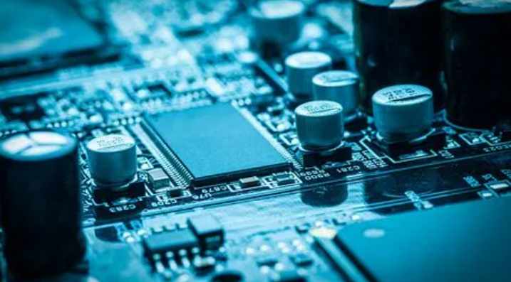
PCB stands for Printed circuit Board. Printed circuit boards, or PCBS, are found in almost every electronic device or gadget you might use in your daily and professional life. PCBS are located at the center of most electronic products and are therefore extremely critical components. It is the component that allows current to flow through the circuit and can then perform or perform the operations and functions of the device.
Given its importance to any electronics you own, here's a little guide to what PCBS are and how they actually form.
What are PCBS?
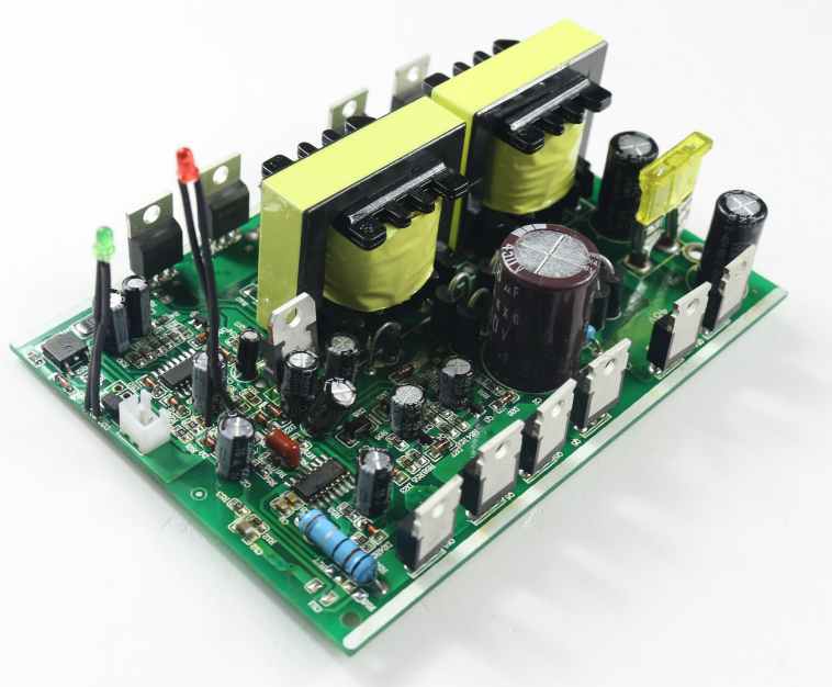
A printed circuit board is essentially a substrate whose role is to support the various electronic components that make up an electronic product and its circuits, allowing current to flow over its surface and powering each individual component in a conductive manner. The circuit is etched onto the surface of the substrate using conductive rails and pads for attaching various components. These components are usually soldered to the circuit board, which provides mechanical support and the basic substrate.

A PCB can also be single, double or even multilayer, depending on the number of copper layers it uses on top of the substrate layer. Which option to use depends on the functionality you need to extract from the PCB. The degree of flexibility and functionality of commonly used circuit boards today far exceeds what was considered standard just a few years ago. As with any other technology, achieving PCBS as we know them today was a gradual process that required a lot of trial, failure, and success. Ultimately, our goal is to create a manufacturing process for PCBS that allows us to incorporate the largest functionality onto the smallest chip. The smaller the technology, the more features, the better.
From 1900 to 1950
In the early 1900s, printed circuit boards were not yet common or widely used. Instead, point-to-point structures were used to create large, bulky designs that were executed on chassis that were essentially wooden or metal bases or frames. They would attach large insulators, regulators and other components to the frame and then connect them to each other with welded wires and connectors. When they do get the job done, they are slow, inefficient, unreliable and extremely fragile, prone to breakdowns that result in countless lost and wasted efforts and labor.
It wasn't until 1903, when Albert Hanson patented a device using insulated boards and multiple layers of arranged foil conductors, that we really started moving toward printed circuit boards. The German conductor also showed how the layers could be punched to achieve electrical connections. Several scientists and leaders in electronics and engineering then began experimenting with ideas to take the concept further. Although significant efforts were made to introduce new and improved electronic devices and appliances to the general market, the development of circuit boards faced a number of obstacles in the form of World Wars and the Great Depression.
In late 1936, Austrian engineer Paul Eisler invented the concept of printed circuit boards using existing printing technology.
1950 to present
Eventually, as part of the effort to begin using proximity fuzes for World War II, the U.S. government adapted the technology for military purposes. More work and development in this area led to the commercialization of printed circuit boards in the mid-1950s.
In this era, the substrates used to make circuit boards included resin and bakelite. A complex process, remarkable speed and efficiency, and a significant reduction in the size of circuit boards are what encouraged inventors to pursue and invest in this technology. The wire pattern will be hand-painted onto the board and photographed onto the zinc plate, which can then be used to print electronic designs. The copper foil will be used as a conductive material and the design will be etched with acid-resistant ink.
In the 1960s and 1970s, as we moved away from the days when we had to drill and punch holes and use wires to create interconnections between the various components on the board, we began to focus our efforts on making PCBS smaller and smaller without compromising the speed or efficiency of the circuit, if not further improving it. This led to the popularity in the 1980s of using surface mount components instead of perforated components. This helps improve functionality while reducing size and cost.
From there, the trend continues to increase the complexity of the board. By the 1990s, multilayer PCBS were introduced to the market, and inventors began to realize the potential behind the technology. As manufacturers began to use microporous technology to produce PCBS that used high-density interconnects, PCBS became smaller and more flexible. This further enables manufacturers to incorporate larger designs onto smaller surfaces.
Now, with 3D printing, it's understandable that the trend of making complex miniature designs on PCBS will continue to grow.
Global PCB Market: Growth, Trends and Forecasts
Feb 01,2023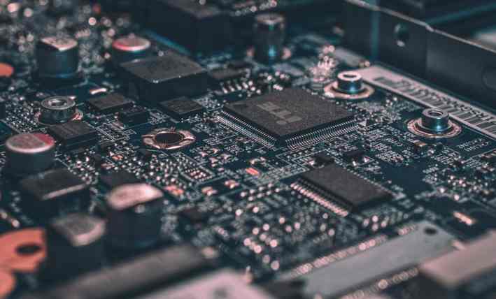


Just upload Gerber files, BOM files and design files, and the KINGFORD team will provide a complete quotation within 24h.