
Professional PCB manufacturing and assembly
Building 6, Zone 3, Yuekang Road,Bao'an District, Shenzhen, China
+86-13410863085Mon.-Sat.08:00-20:00

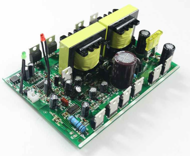
Perforation is one of the important components of multilayer PCB board, and the cost of drilling usually accounts for 30% to 40% of the cost of PCB board. Simply put, every hole in the PCB can be called a pass hole.
I. Parasitic capacitance through the hole
There is a parasitic capacitance to the ground through the hole itself. If the diameter of the isolation hole through the hole on the paving layer is D2, the diameter of the welding plate through the hole is D1, the thickness of the printed circuit board is T, and the dielectric constant of the substrate is ε, then the parasitic capacitance through the hole is approximately as follows: C= 1.4epsilon TD1/(D2-D1) The main effect of the parasitic capacitance through the hole on the circuit is to prolong the signal rise time and reduce the speed of the circuit. For example, for a PCB board with a thickness of 50Mil, if a through-hole with an inner diameter of 10Mil, a diameter of 20Mil of the pad is used, and the distance between the pad and the copper floor area is 32Mil, then we can approximate the parasitic capacitance of the through-hole through the above formula: C=1.41x4.4x0.050x0.020/(0.032-0.020)=0.517pF, the rise time change caused by this part of capacitance is: T10-90=2.2C(Z0/2)=2.2x0.517x(55/2)=31.28ps. It can be seen from these values that although the effect of the parasitic capacitance of a single hole is not obvious, the designer should be careful if multiple holes are used to switch between layers in the route.
Two, the parasitic inductance through the hole
Similarly, there is also a parasitic inductance when there is a parasitic capacitance through the hole. In the design of high-speed digital circuits, the harm caused by the parasitic inductance through the hole is often greater than the influence of the parasitic capacitance. Its parasitic series inductance will weaken the contribution of the bypass capacitance and reduce the filtering effectiveness of the whole power system. We can simply calculate the parasitic inductance of a through-hole approximation using the following formula: L=5.08h[ln(4h/d)+1] where L refers to the inductance of the through-hole, h is the length of the through-hole, and d is the diameter of the central borehole. It can be seen from the formula that the diameter of the through hole has little influence on the inductance, while the length of the through hole has the biggest influence on the inductance. Using the above example again, the out-of-hole inductance can be calculated as L=5.08x0.050[ln(4x050/0.010)+1]=1.015nH. If the rise time of the signal is 1ns, the equivalent impedance is XL=πL/T10-90=3.19Ω. Such impedance can no longer be ignored in the presence of high frequency current. In particular, note that the bypass capacitor needs to pass through two holes when connecting the power layer to the formation, so that the parasitic inductance of the holes will be multiplied.
3, high speed PCB hole design
Through the above analysis of the parasitic characteristics of the holes, we can see that in high-speed PCB design, seemingly simple holes often bring great negative effects to the circuit design. In order to reduce the adverse effects brought by the parasitic effect of the hole, the design can be as far as possible:

1, from the cost and signal quality, choose a reasonable size of the hole. For example, for the design of 6-10 layers of memory module PCB, it is better to choose 10/20Mil(drill/pad) pass hole, for some high-density small size boards, you can also try to use 8/18Mil pass hole. With current technology, it is difficult to use smaller holes. For the power supply or ground wire hole can be considered to use a larger size, to reduce the impedance.
2. From the two formulas discussed above, it can be concluded that the use of thinner PCB board is beneficial to reduce the two parasitic parameters through the hole.
3. The pins of the power supply and the ground should be drilled nearby. The shorter the lead between the pins and the holes, the better, because they will lead to the increase of inductance. At the same time, power and ground leads should be as thick as possible to reduce impedance.
4, the signal on the PCB board should not change the layer as far as possible, that is to say, try not to use unnecessary holes.
5. Place some grounded holes near the holes of the signal changing layer in order to provide the nearest loop for the signal. You can even put a lot of extra ground holes on the PCB circuit board. Of course, you need to be flexible in your design. The perforated model discussed above is the case that each layer has pads, and sometimes, we can reduce or even remove the pads of some layers. Especially in the case of very large pore density, it may lead to the formation of a fault slot that cuts off the circuit in the copper layer. To solve this problem, in addition to moving the position of the hole, we can also consider reducing the size of the solder pad in the copper layer


Just upload Gerber files, BOM files and design files, and the KINGFORD team will provide a complete quotation within 24h.