
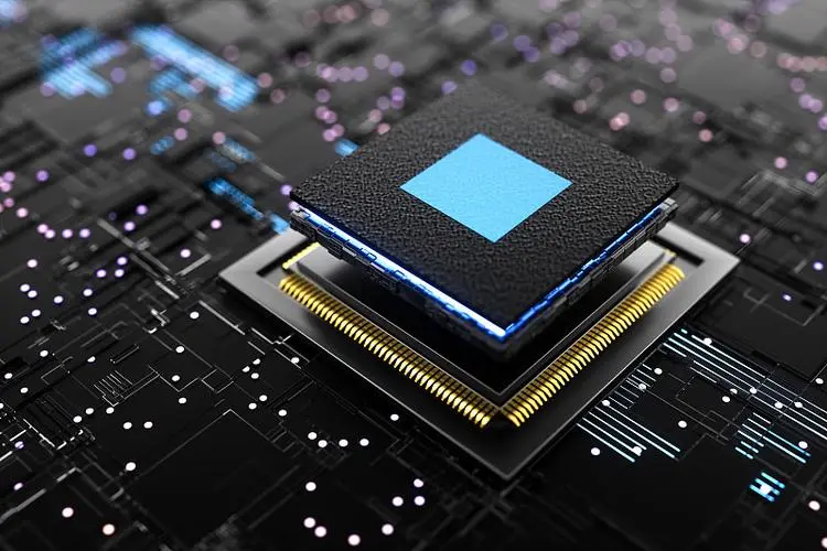
Professional PCB manufacturing and assembly
Building 6, Zone 3, Yuekang Road,Bao'an District, Shenzhen, China
+86-13410863085Mon.-Sat.08:00-20:00


1. The flow direction should be scientific and reasonable
This point involves a lot of aspects, such as high pressure, low pressure, input, output, strong and weak data signals, high frequency, low frequency and so on. Their flow should most reasonably be linear and should not merge with each other. It follows the principle of eliminating dry scratching between each other. A more suitable flow is in a straight line, but it is difficult to achieve. The worst direction is a loop, and thankfully there is an isolation operation. Low voltage PCB design requirements can be lower if it is specifically aimed at DC. So what is called "scientifically sound" is relative.
2. The layout of power filtering and decoupling capacitors is reasonable
The layout of PCB circuit board is critical to the appearance and performance of the entire circuit board. Only part of the power filter and decoupling capacitors are shown in the schematic, but it is not specified where they are connected. I think those capacitors are for switching devices or other components that need to be filtered and decoupled, the position of the capacitor should be against those components, and the effect will not be found at a distance. When we scientifically filter the power supply and decouple the capacitor, common problems with ground points no longer seem to be prominent.
3. Good ground point
I don't need to tell you how important it is to pick a landing spot. It has been discussed by countless professionals and generally requires standard common ground. For example, the multiple ground lines of the forward amplifier should be combined and then connected to the main line, and so on. However, in real life, due to various types of restrictions, it is difficult to complete. But we should not ignore it and do our best to follow the principles. This common problem is very flexible in practice, and different people have different solutions. If you can specifically for specific pcb circuit boards to express it is very easy to understand.
4. Reasonable line selection
Call the circuit board, line is of course very important drop! Make the line as wide as possible. High voltage and high frequency lines should be smooth, no sharp chamfer. At the bend should not be 90 degrees, the ground should be as wide as possible. Want to solve the problem of ground point, a better way is to cover a large area of copper. If there's a better way, please leave a comment in the comments section and I'll learn more.
The problem of PCB circuit board is closely related to design and circuit board processing. For example, sometimes the problems in post-production may be caused by the design of PCB circuit boards. For example, too many line holes, substandard copper sinking process and so on are easy to hide a lot of safety risks. From the above problems, we can draw a conclusion that in the design of PCB circuit boards should be as much as possible to reduce the hole through the line. If the number of parallel lines in the same direction is large and dense, they will be joined together during welding. Therefore, the welding level determines the linear density during production. The spacing of solder joints is too small, the difficulty of manual welding is increased a lot, then the only way to solve the welding quality - to reduce the efficiency. Otherwise the problems will pile up and get harder to deal with. The level and efficiency of the welder determines the narrowest spacing of solder joints.
When the pad or through the hole size is too small, it is more difficult for manual drilling. When the size of the pad does not match the size of the hole, it is a bolt from the blue for CNC drilling, and the pad is easy to take the shape of the C word. The pads could have been drilled out in serious cases. If the wires are too thin, and there is no copper in the large unwired area, the corrosion is likely to be uneven. That is to say, when the corrosion of the unwired area, it is likely to be excessive corrosion of the fine wire. Sometimes it looks like the wire is broken but it's not, and in the worst cases it's broken. Therefore, the setting of copper is not only to expand the ground area.
Shenzhen PCB proofing price
Feb 01,2023


Just upload Gerber files, BOM files and design files, and the KINGFORD team will provide a complete quotation within 24h.