
Professional PCB manufacturing and assembly
Building 6, Zone 3, Yuekang Road,Bao'an District, Shenzhen, China
+86-13410863085Mon.-Sat.08:00-20:00

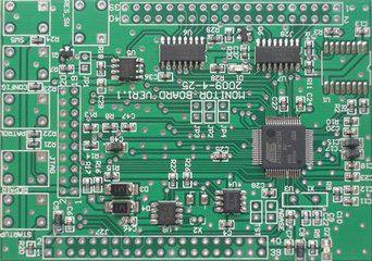
Introduction to solder resistance layer
Solder pad refers to the part of the board to be coated with green oil. In fact, the solder mask uses a negative output, so when the shape of the solder mask is mapped to the board, it is not green oil solder, but exposed copper. Usually in order to increase the thickness of copper, the welding resistance layer is marked to remove green oil, and then tin is added to increase the thickness of copper wire.
Welding resistance layer requirements
Choke layers are important in controlling weld defects in reflow welding, and PCB designers should minimize spacing or air gaps around the pads.

While many process engineers would prefer a solder shield to separate all pad features on the plate, pin spacing and pad size for closely spaced components will require special consideration. While non-zoned solder layer openings or Windows on the four sides of the qfp may be acceptable, controlling the tin bridge between the element pins may be more difficult. For bga solder shields, many companies offer a solder shield that does not touch the pad, but covers any features between the pads to prevent tin Bridges. Most surface mounted PCB board are covered with solder resistance layer, but solder resistance coating, if thickness is greater than 0.04mm, may affect solder paste application. Surface-mounted PCB, especially those using closely spaced components, require a low photoresist layer.
Job production
Solder resistance materials must be used by liquid wet process or dry film lamination. Dry film solder resistance material is available in 0.07-0.1mm thicknesses and is suitable for some surface mount products, but this material is not recommended for close spaced applications. Few companies offer dry films thin enough to meet tight spacing standards, but several companies offer liquid sensitive solder resistance materials. Normally, the choke opening should be 0.15mm larger than the pad. This allows a 0.07mm gap on the side of the pad. Low-profile liquid photosolder materials are economical and are often specified for surface mount applications, providing precise feature sizes and clearances.
Introduction of welding aid layer
The welding aid layer is used for patch encapsulation, corresponding to the patch component pad. In SMT processing, a steel plate is usually used to punch holes on the PCB corresponding to the solder pad of components, and then the solder paste on the steel plate. When the PCB is under the steel plate, the solder paste leaks down, which means that each solder pad can be stained with solder, so usually the solder resistance layer cannot be larger than the actual size of the solder pad, and it is better to be less than or equal to the actual size of the solder pad.
The required level and sticker elements are almost the same, and the main requirements are as follows:
1. BeginLayer: ThermalRelief and AnTIPad should be 0.5mm larger than the actual size of the regular pad
2. EndLayer: ThermalRelief and AnTIPad should be 0.5mm larger than the actual size of the regular pad
3. DEFAULTINTERNAL: Intermediate layer
The role of solder shield and solder aid
Solder resistance layer is mainly to prevent PCB copper foil directly exposed to the air, play a protective role.
The welding layer is used to make steel mesh for the steel mesh factory, and the steel mesh can be accurately placed on the solder paste to be welded on the patch pad.
Difference between printed circuit board welding aid layer and welding resistance layer
The two layers are used for soldering on tin, not a tin, a green oil;
1. The welding resistance layer means that the window is opened on the green oil of the whole piece of welding resistance, in order to allow welding;
2. By default, green oil should be applied to areas without solder resistance layer;
3. Welding aid layer is used for patch encapsulation


Just upload Gerber files, BOM files and design files, and the KINGFORD team will provide a complete quotation within 24h.