
Professional PCB manufacturing and assembly
Building 6, Zone 3, Yuekang Road,Bao'an District, Shenzhen, China
+86-13410863085Mon.-Sat.08:00-20:00


Chip thrust test and through-hole technology
Standard method and precautions for patch thrust test
Some precautions and methods must be paid attention to during the thrust test of the patch assembly. The purpose of the toilet is to test the welding fastness and adhesion strength of the patch assembly.
1. Precautions for thrust test of SMT patch assembly:
1. Do not apply force quickly during measurement to avoid damaging the device;
2. The thrust test standards of different devices are not specified by the customer, but can be implemented by referring to relevant quality standards or IPC general inspection standards.
2. Thrust test method of SMT chip assembly:
1. After the production line is transferred to the production line, IPQC needs to conduct adhesion thrust test of SMD components, and use a thrust meter to test components of different specifications on PCBA. Before the thrust test, it is necessary to reset the thrust gauge to zero so that the pointer points to "0". "Scale;
Circuit board

2. The use of thrust time calculation requires that the thrust meter and the measured data apply force at an angle of 30 ° to 45 °, and the force can reach the specified standard requirements at a uniform speed;
3. The excellent and non excellent products tested shall be recorded on the corresponding inspection record sheet;
4. After the test, unqualified products must be placed separately, and can be removed after maintenance and re inspection;
3. Thrust test standard of SMT chip assembly:
10603 is greater than 0.8KG
20805 is greater than 1.0KG
3.1206 is greater than 1.5KG
4. Diode larger than 1.5KG
5. The transistor element is larger than 2.0KG
6. IC chip larger than 3.0KG
7. The use of thrust time calculation requires that the thrust meter and measured data shall be applied at an angle of 30 ° to 45 °, and the force can be obtained at a uniform speed, meeting the above specified standard requirements.
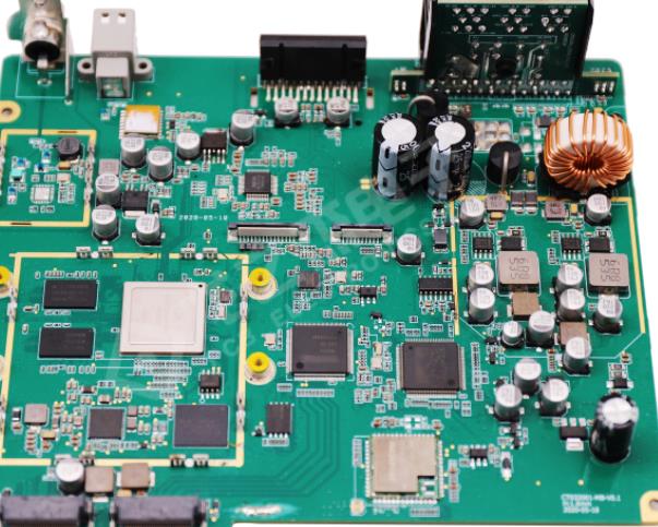
The emergence of SMT chip and through-hole technology
Surface mount technology is a part of electronic components, which is responsible for installing electronic components on the surface of PCB. The electronic components installed in such pipes are called surface mounted devices (SMDs). The purpose of developing surface mount technology is to effectively use PCB space while minimizing manufacturing costs. The introduction of surface mount technology allows PCB design services for highly complex electronic circuits with smaller components. This paper will discuss the advantages and disadvantages of SMT.
The emergence of SMT chip and through-hole technology
Surface mount technology developed in the 1960s and was widely used in the 1980s. By the 1990s, they had been used for most high-end PCB components. Traditional electronic components have been redesigned to include metal lugs or end caps that can be connected directly to the surface of the circuit board. This replaces the typical wire that needs to be drilled through. Compared with through hole mounting, surface mount can make components smaller, and components can be placed on both sides of the circuit board more frequently. SMT can achieve a higher degree of automation, thereby minimizing labor costs, improving productivity, and achieving advanced PCB design and development.
The following are the salient features of SMT and through-hole technology:
Surface Mount Technology (SMT)
SMT allows power components to be mounted on the PCB surface without any drilling. These components have smaller or no leads at all, and are smaller than through hole components. Since surface mount components do not require a lot of drilling, they are more compact and suitable for higher wiring density.
Through hole technology
Over the years, almost all PCB circuit boards have adopted through-hole technology This installation involves inserting the leads of electronic components into the holes drilled on the PCB, and then welding them to the pads on the other side of the PCB Because through hole installation provides a firm mechanical combination, it is very reliable However, drilling PCB in the production process often increases manufacturing costs In addition, SMT via technology limits the wiring area of the signal trace below the top layer of the multilayer board


Just upload Gerber files, BOM files and design files, and the KINGFORD team will provide a complete quotation within 24h.