
Professional PCB manufacturing and assembly
Building 6, Zone 3, Yuekang Road,Bao'an District, Shenzhen, China
+86-13410863085Mon.-Sat.08:00-20:00


SMT machining surface assembly process
Inspection Methods for SMT Machined Surface Assembly Process
The commonly used inspection methods in surface assembly mainly include manual visual inspection, non-contact inspection and contact inspection. Visual inspection mainly uses magnifying glass, binocular microscope, 3D rotating microscope, projector, etc.; Non contact testing mainly adopts automatic optical testing (AOI) and automatic X-ray testing (AXI); Contact test is mainly used for circuit test (circuit test, ICT), flying probe test (flying probe test, FPT), functional test (functional test, FT), etc. Because the content and characteristics of each process are different, the detection methods used in each process are also different. Among the above inspection methods, manual visual inspection, automatic optical inspection and X-ray inspection are the three most commonly used methods in surface assembly process inspection.
1) Manual visual inspection method
This method requires little investment and does not require the development of test programs, but it is slow and subjective and requires visual observation of the test area Due to the lack of visual inspection, it is rarely used as the main welding quality inspection method in the current SMT production line, and mostly used for repair and rework With miniaturization, fine spacing and assembly density of components, direct visual inspection becomes more and more difficult, even impossible For example, if the current is 0201.01005, the welding quality cannot be judged by naked eyes Therefore, most of them need various optical magnifiers and special optical instruments Typical examples include VPI.OK of microscope from ERSA, Germany, and related products from Christie's and other companies in the United States With the help of these products, on the one hand, we can not only check the surface adhesion technology to complete the seam, but also observe the hidden solder joint detection of BGA and other array devices to a certain extent, which cannot be completed through direct visual inspection; On the other hand, it has measurement function, even video function, so that it can be popularized and applied in process research and development and defect diagnosis
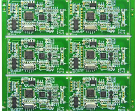
Circuit board

2) Automatic optical inspection method
With the decrease of component package size and the increase of chip density of circuit board, the inspection of shape memory alloy becomes more and more difficult, and manual visual inspection seems insufficient. Its stability and reliability are difficult to meet the needs of production and quality control. The use of automatic detection has become increasingly important. The use of automatic optical inspection (AOI) as a tool to reduce defects can detect and eliminate errors early in the assembly process to achieve good process control. AOI adopts advanced vision system, new luminous methods, high magnification and complex processing methods to achieve high defect capture rate at high test speed. AOI system can check most components, including rectangular chip components, cylindrical components, button electrolytic capacitors, transistors, PLCC, QFP, etc. It can detect missing components, polarity errors, installed solder offset, excessive or insufficient solder, solder bridge, etc., but cannot detect circuit errors. At the same time, it cannot detect invisible solder joints.
(1) The position of AOI on the SMT production line There are usually three types of AOI equipment PCBA production line
1. AOI used to detect solder paste failure after screen printing is called AOI after screen printing.
2. The AOI placed after the placement to detect the device placement failure is called the post attachment A0Io
3. AOI used to detect equipment installation and welding faults after reflow is called A0Io after reflow, which is an example of using AOI to detect defects after reflow.
(2) AOI inspection process. AOI detection is one of the most commonly used detection methods in SMT.
1. Production preparation includes machine preparation, PCB preparation for inspection, file preparation, importing Gerber files, etc.
2. The parameter setting includes programming the standard board. You can use the assembly library or customize it, use the customized framework to set the framework for the assembly, enter the assembly type, and set the threshold, upper limit, lower limit and other information.
3. Contour selection includes automatically acquiring printing solder paste, patch and solder joint images by controlling light source and other A0I; The corresponding image processing is carried out by applying image processing algorithm; Get contour information of printing pastes, components and solder joints.
Inspection of components after SMT chip assembly
Dec 01,2022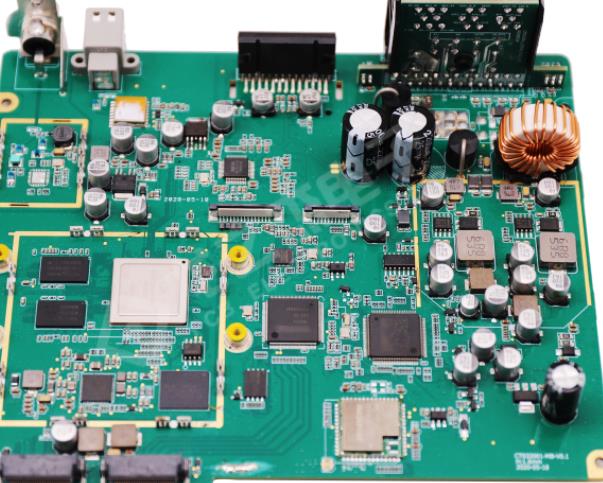


Just upload Gerber files, BOM files and design files, and the KINGFORD team will provide a complete quotation within 24h.