
Professional PCB manufacturing and assembly
Building 6, Zone 3, Yuekang Road,Bao'an District, Shenzhen, China
+86-13410863085Mon.-Sat.08:00-20:00

The embodiment of horizontal electroplating in PCB process
PCB manufacturing, PCB design and PCBA processing manufacturers explain the embodiment of horizontal electroplating in PCB process
The design of printed circuit board is based on the circuit schematic diagram to realize the functions required by the circuit designer. The design of printed circuit board mainly refers to layout design, which needs to consider the layout of external connections. The optimal layout of internal electronic components, the optimal layout of metal wiring and through-hole, electromagnetic protection, heat dissipation and other factors. Excellent layout design can save production costs and achieve good circuit performance and heat dissipation.
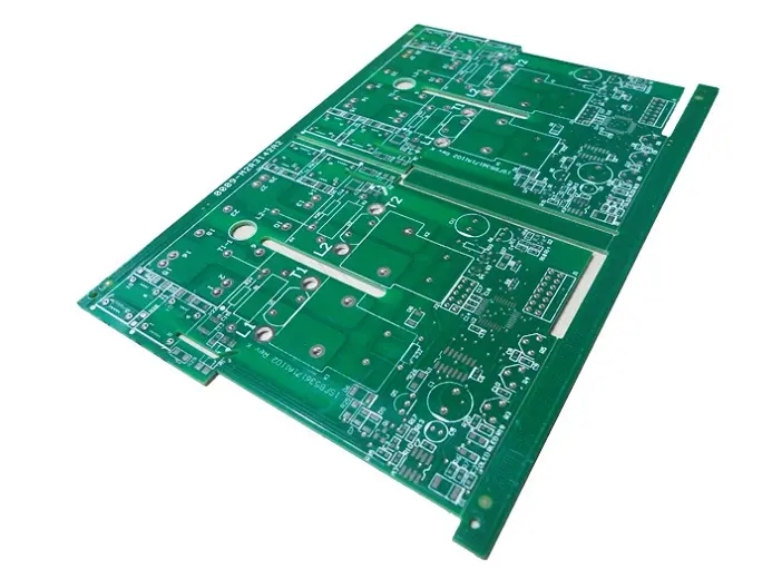
PCB manufacturing is developing rapidly in the direction of multilayer, lamination, functionality and integration. With the rapid development of microelectronics technology, the concept and design of printed circuit graphics are promoted by using a large number of micro holes, narrow spacing and thin wires in printed circuit design. It makes PCB manufacturing technology more difficult, especially the aspect ratio of the through holes of the multilayer board exceeds 5:1 and the deep blind holes are widely used in the laminate, which makes the conventional vertical electroplating process unable to meet the technical requirements of high-quality and high reliability interconnection holes. The main reason is to analyze the current distribution state from the electroplating principle. Through actual electroplating, it is found that the current distribution in the hole presents a waist drum shape, and the current distribution in the hole gradually decreases from the hole edge to the hole center, resulting in a large amount of copper deposition on the surface and the hole edge. It is impossible to ensure that the copper layer in the hole center should reach the specified thickness. Sometimes the copper layer is extremely thin or there is no copper layer, which will cause irreparable loss in serious cases, A large number of multilayer boards were scrapped. In order to solve the product quality problem in mass production, the current and additives are used to solve the deep hole electroplating problem.

In the copper electroplating process for high aspect ratio PCB, most of them are assisted by high-quality additives, combined with moderate air agitation and cathode movement, to enlarge the electrode reaction control area in the hole under relatively low current density, so that the role of electroplating additives can be shown. In addition, the cathode movement is very conducive to the improvement of the deep plating ability of the plating solution, and the polarization of the plating piece is increased, In the process of electrodeposition, the formation rate of crystal nucleus and the growth rate of grains compensate each other, thus obtaining a high toughness copper layer.
However, when the aspect ratio of through-hole continues to increase or deep blind holes appear, these two process measures are weak. A horizontal plating technique occurs. The continuous development of vertical electroplating technology is a new electroplating technology developed on the basis of vertical electroplating technology. The key of this technology is to create an appropriate and complementary horizontal electroplating system, which can enable the plating solution with high dispersion capacity, improve the power supply mode and cooperate with other auxiliary devices to display more excellent functions than the vertical electroplating method. PCB manufacturing, PCB design and PCBA processing manufacturers will explain the embodiment of horizontal electroplating in PCB process.


Just upload Gerber files, BOM files and design files, and the KINGFORD team will provide a complete quotation within 24h.