
Professional PCB manufacturing and assembly
Building 6, Zone 3, Yuekang Road,Bao'an District, Shenzhen, China
+86-13410863085Mon.-Sat.08:00-20:00

What HDI boards are introduced by circuit board manufacturers
The circuit board manufacturer, circuit board design and PCBA processing manufacturer explain to you: what is HDI board introduced by the circuit board manufacturer, HDI circuit board introduced, explained
Printed circuit board is a structural component formed by insulating materials and conductor wiring. When the final product is made, integrated circuits, transistors, diodes, passive components (such as resistors, capacitors, connectors, etc.) and other various electronic parts will be installed on it. Through wire connection, electronic signal connection and proper function can be formed. Therefore, the printed circuit board is a platform to provide component connection, which is used to undertake the basis of connecting parts.
As printed circuit board is not a general end product, the definition of its name is slightly confused. For example, the motherboard for personal computers is called the motherboard and cannot be directly called the circuit board. Although there are circuit boards in the motherboard, they are not the same. Therefore, when evaluating the industry, they cannot be said to be the same. Another example: because there are integrated circuit parts loaded on the circuit board, the news media call it IC board, but in fact it is not the same as printed circuit board.

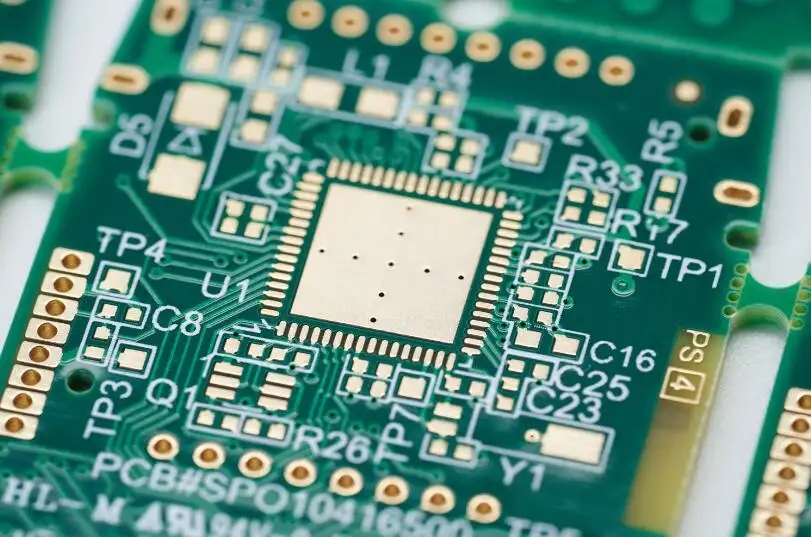
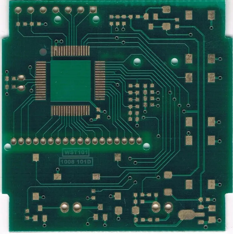
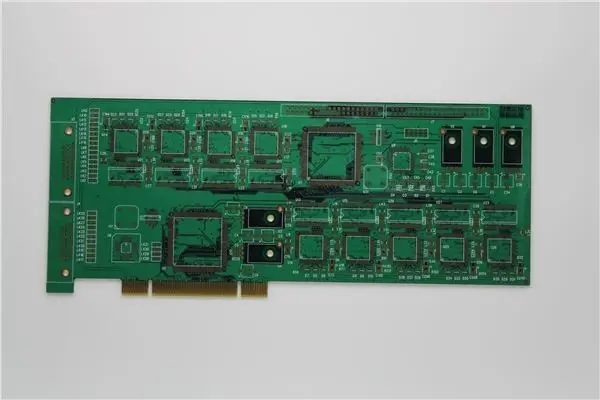
Under the premise that electronic products tend to be multi-functional and complex, the contact distance of integrated circuit components will be reduced, and the speed of signal transmission will be relatively improved, followed by an increase in the number of wiring and a local reduction in the length of wiring between points. These require the application of high-density wiring configuration and microporous technology to achieve the goal. Wiring and jumper are basically difficult for single and double sided boards. As a result, the circuit board will move towards multilayer. With the continuous increase of signal lines, more power layers and ground layers are necessary for design. All of these make the multilayer printed circuit board more common.
For the electrical requirements of high-speed signals, the circuit board must provide impedance control with AC characteristics, high-frequency transmission capability, and reduce unnecessary radiation (EMI). With the structure of Stripline and Microstrip, multi-layer design becomes necessary. In order to reduce the quality problem of signal transmission, insulating materials with low dielectric coefficient and low attenuation rate will be used. In order to meet the miniaturization and array of electronic components, the density of circuit boards will also be continuously increased to meet the needs. The appearance of BGA (Ball Grid Array), CSP (Chip Scale Package), DCA (Direct Chip Attachment) and other assembly methods of group parts has pushed the printed circuit board to an unprecedented high-density state.
All holes with a diameter less than 150um are called micro vias in the industry. Circuits made by using the geometric structure technology of such micro holes can improve the efficiency of assembly, space utilization, etc., and are also necessary for the miniaturization of electronic products.
For circuit board products with this structure, there have been many different names in the industry to call such circuit boards. For example, European and American companies used to call this kind of product SBU (Sequence Build Up Process), which is generally translated as "sequential layer adding method", because the program they produced used a sequential construction method. As for Japanese manufacturers, because the pore structure produced by such products is much smaller than that in the past, the manufacturing technology of such products is called MVP (Micro Via Process), which is generally translated as "microporous process". Some people also call this kind of circuit board BUM (Build Up Multilayer Board) because the traditional multilayer board is called MLB (Multilayer Board), which is generally translated as "layered multilayer board".
In order to avoid confusion, the IPC Board Association of the United States proposed to call such products HDI (High Density Interconnection Technology), which would become high-density connection technology if translated directly. However, this cannot reflect the characteristics of the circuit board. Therefore, most circuit board manufacturers refer to such products as HDI boards or the full Chinese name "high-density interconnection technology". However, because of the problem of oral fluency, some people directly call such products "high-density circuit boards" or HDI boards.


Just upload Gerber files, BOM files and design files, and the KINGFORD team will provide a complete quotation within 24h.