
Professional PCB manufacturing and assembly
Building 6, Zone 3, Yuekang Road,Bao'an District, Shenzhen, China
+86-13410863085Mon.-Sat.08:00-20:00

Design of Power Supply Circuit for Power Receiving Unit of Wireless Charging PCB Board
After the electric energy is received through the coil voltage reduction, the high-frequency AC voltage passes through the IN4007 rectifier tube for full wave rectification, 2200uf capacitor filtering, and then the 3.3V regulator diode wakes up to stabilize the voltage. The output DC power provides a relatively stable working voltage for the battery to charge it.
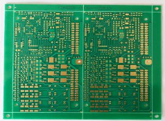
Wireless charging PCB board
Overall power of wireless charging PCB board
The basic function of the wireless charger is to transmit H electric energy H to the battery in H wireless H mode through the coil. Just put the battery and receiving device on the charging platform to charge them. The experiment proves that although the system can not be charged invisibly, it can place multiple calibration devices on the same charging platform for simultaneous charging. Avoid the trouble of wiring.
1 Principle and structure of wireless charger
The wireless charging system mainly adopts the principle of electromagnetic induction, and realizes energy transmission through energy coupling of coils. When the wireless charging PCB board system is working, the input terminal converts the AC mains power into DC through the full bridge rectifier circuit, or uses the 24V DC terminal to directly supply power to the system. The DC output from the H power management H module is converted into high-frequency AC power through 2M active crystal oscillator inverter to supply the primary winding. The energy is coupled through two H inductors and H coils, and the current output from the secondary coil is changed into DC through the receiving conversion circuit to charge the battery.
2 Power management of wireless charging PCB board
3 Wireless charging PCB transmitting circuit module
The main oscillator circuit uses a 2MHz active crystal oscillator as the oscillator. The square wave output by the active crystal oscillator is filtered out by the second-order low-pass filter to obtain a stable sine wave output. It is output to the parallel resonant circuit composed of PCB coil and capacitor for radiation after passing through the Class C amplifier circuit composed of the triode 13003 and its peripheral circuits to provide energy for the receiving part.
4 Wireless charging PCB board receiving circuit module and charging circuit
It is measured that the wire diameter of the air core coupling coil of the parallel resonant circuit composed of capacitors is 0.5 mm, the diameter is 7 cm, the inductance is 47 uH, and the carrier frequency is 2 MHz. According to the parallel resonance formula, the matching capacitance C is about 140 pF. Therefore, 2MHz active crystal oscillator is used in the transmitting part to generate the energy carrier frequency close to the resonant frequency.


Just upload Gerber files, BOM files and design files, and the KINGFORD team will provide a complete quotation within 24h.