
Professional PCB manufacturing and assembly
Building 6, Zone 3, Yuekang Road,Bao'an District, Shenzhen, China
+86-13410863085Mon.-Sat.08:00-20:00

Explanation of the development history of PCB substrate materials
The development of PCB substrate materials has gone through nearly 50 years. In addition, there were about 50 years of scientific experiments and exploration on the basic raw materials used in this industry - resin and reinforcement materials before the industry was determined. PCB substrate materials have accumulated nearly a hundred years of history. The development of substrate material industry at each stage is driven by the innovation of electronic complete machine products, semiconductor manufacturing technology, electronic installation technology, and electronic circuit manufacturing technology. From the beginning of the 20th century to the end of the 1940s, it was the embryonic stage of PCB substrate material industry. Its development features are as follows: at this time, a large number of resins, reinforcement materials and insulating substrates for substrate materials emerged, and the technology was initially explored. All these have created the necessary conditions for the emergence and development of the most typical substrate material for printed circuit boards - copper clad laminate. On the other hand, PCB manufacturing technology with metal foil etching (subtraction) as the mainstream has been initially established and developed. It plays a decisive role in determining the structural composition and characteristic conditions of CCL.
Copper clad laminate was really adopted in PCB production on a large scale. It first appeared in the American PCB industry in 1947. Therefore, PCB substrate material industry has entered its initial development stage. In this stage, the progress of manufacturing technology of raw materials used in the manufacture of substrate materials - organic resin, reinforcement materials, copper foil, etc., has given a strong impetus to the progress of substrate material industry. Because of this, the substrate material manufacturing technology has become mature step by step.
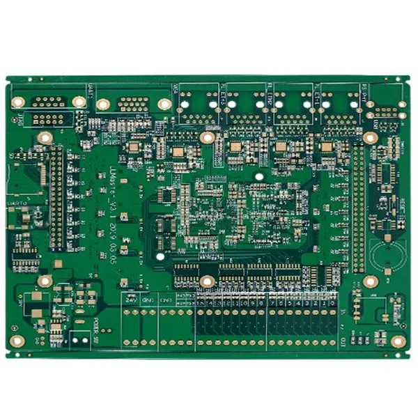
PCB base plate - copper clad plate
The invention and application of integrated circuits and the miniaturization and high-performance of electronic products have pushed the PCB substrate material technology onto the track of high-performance development. With the rapid expansion of demand for PCB products in the world market, the output, variety and technology of PCB substrate materials have been developed at a high speed. At this stage, a broad new field of substrate materials application - multilayer printed circuit board has emerged. At the same time, the structural composition of substrate materials at this stage has further developed its diversification. At the end of the 1980s, portable electronic products represented by notebook computers, mobile phones and small video cameras began to enter the market. These electronic products are rapidly developing towards miniaturization, lightweight and multi-function, which has greatly promoted the progress of PCB towards micro holes and micro wires. With the above changes in PCB market demand, a new generation of multilayer boards that can realize high-density wiring, called built-up multilayer boards (BUM), came out in the 1990s. The breakthrough of this important technology has also made the substrate material industry enter a new stage of development dominated by substrate materials for high-density interconnection (HDI) multilayer boards. In this new stage, the traditional CCL technology is facing new challenges. PCB substrate materials have undergone new changes and innovations in terms of manufacturing materials, production varieties, organizational structure and performance characteristics of substrate, as well as product functions.
Relevant data show that the output of rigid copper clad laminate in the world increased at an average annual rate of about 8.0% in the 12 years from 1992 to 2003. In 2003, the total annual output of rigid copper clad laminate in China has reached 105.9 million square meters, accounting for 23.2% of the global total. The sales revenue reached 6.15 billion US dollars, the market capacity reached 141.7 million square meters, and the production capacity reached 155.8 million square meters. All these indicate that China has become the "superpower" in the world of CCL manufacturing and consumption
PCB manufacturers, PCB designers and PCBA manufacturers will explain the development of PCB substrate materials.


Just upload Gerber files, BOM files and design files, and the KINGFORD team will provide a complete quotation within 24h.