
Professional PCB manufacturing and assembly
Building 6, Zone 3, Yuekang Road,Bao'an District, Shenzhen, China
+86-13410863085Mon.-Sat.08:00-20:00


In addition to schematic design done by hardware engineers and PCB layout, layering and wiring design done by pcb engineers, structural engineers should not only participate in the design at the beginning, but also plan and constrain the size, shape, installation mode, installation hole location and number of boards to form drawing documents, The board design file output by the hardware engineer and the pcb engineer is an input condition file for each other, and the design process is iterated repeatedly until the production version file of the board is finally determined.
Some key points of PCB design in this process are summarized as follows:
Board size and shape
The size of the board is determined by two factors: one is the size of the whole equipment; The second is the functional principle design of the board. For example, a board needs a certain number and type of components to achieve a certain function. The size of these components sets a basic requirement for the size of the board. If the size of the board is small, these components cannot be placed.
If there are standard requirements for the shape of the board, follow the standard. For example, the size of the 3U plug-in board of the standard VPX bus is 100mm * 160mm, and the size of the 6U plug-in board is 233.35mm * 160mm. If it is a non-standard board, the board shape can be determined by combining the shape of the chassis or cold plate.
Mounting hole
The installation holes shall be arranged evenly as far as possible, and the spacing between holes is generally designed to be about 40mm, so as to improve the rigidity of the board and the uniform force.
Connector, guide sleeve/pin position
The position of the connector between the board and the motherboard or backplane shall be in accordance with the relevant standards. If the connector itself does not have a guide device, the guide device needs to be designed on the sub board and the backplane respectively. For example, the cpci connector has its own guiding device, while the vpx connector has no guiding device.
Location and installation of external connectors
The position of the external interface connector from the board depends on a. the size of the connector itself, b Chassis wall thickness. The local wall thickness of the chassis here shall also consider the spacing requirements of connector plugs and sockets.
The installation of connector shall depend on whether it is equipped with mounting bracket and mounting hole. If not, a mounting bracket shall be designed structurally for the purpose of a. fixing the connector and b. as the tooling for connector welding to ensure the accuracy of its welding height.
The spacing of connectors shall be such that there is no interference when plugs are inserted, and a certain operating space shall be reserved. When placing the connector, try to make the direction of 1 pin uniform.
Location of the power socket on the board
The power socket on the board is generally designed for two purposes. One is used as the power input for board debugging, and the other is to provide power for the cooling fan.
The position of the power socket shall be considered structurally, which is generally placed at the edge of the board. If the heat dissipation method of the board is to install an integral cold plate, the power socket shall be provided with an escape hole at the corresponding position of the cold plate. If the debugging power socket is not easy to arrange on the front of the board, you can ask the hardware engineer to place it on the back of the board. The power socket of the fan is close to the fan.
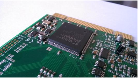
Circuit board
Board locating hole
If the installation accuracy of the board is required to be very high, the positioning holes of the structure can be designed on the board, and the requirements for metallized pads are not necessary.
Device height limit requirements
If there are height limit requirements for components in some areas on the board, they should be marked in the drawing. For example, within the stroke area of self-made non-standard puller, the height of components should not interfere with the handle of the puller.
If the socket on the board needs cold plate opening, whether the opening size is too large and whether it affects the layout of cold plate reinforcement.
In addition to the electrical safety distance, the location of components and parts for dispensing shall also be considered, especially considering the fluidity of the adhesive, and shall not cover the bonding pad of the mounting hole and other areas with overlapping surfaces with the structure.
Whether there are cables on the board, if there are cables, it is necessary to reserve binding holes on the board, and consider whether the bending radius of the cable, the smooth routing, whether there is interference with other components, whether the length of the cable reserves the allowance for assembly and disassembly, etc.
PCB components with high heat generation should be placed close to the cold end of the heat dissipation path. When reviewing the layout of pcb, heat dissipation should be given priority.
Try to use surface mount devices to improve the resistance of the board.
Copper laying requirements, such as the area where cold plates are installed on both sides of the board, the copper laying rate is an important factor affecting the thermal conductivity in the plane direction of the board.
The thickness of the standard plug plate is generally 1.6mm; The thickness of non-standard boards depends on the number of layers and size of boards.
Prohibited cloth requirements, overlapping areas with structural members; The mounting hole requires that the size of the metal pad should be larger than the outer diameter of the flat washer.


Just upload Gerber files, BOM files and design files, and the KINGFORD team will provide a complete quotation within 24h.