
Professional PCB manufacturing and assembly
Building 6, Zone 3, Yuekang Road,Bao'an District, Shenzhen, China
+86-13410863085Mon.-Sat.08:00-20:00

When PCBA is welded, there are usually many requirements for PCBA plates, and the plates must meet the requirements before they can be welded. So why are there so many requirements for plates during welding? It turns out that during the processing of PCBA, there will be many special processes, and the application of special processes will immediately bring about the requirements for PCB boards. If there are problems with PCB boards, it will increase the difficulty of PCBA welding process, which may eventually lead to welding defects, unqualified boards and other situations. Therefore, in order to ensure the smooth completion of processing and facilitate PCBA welding processing, PCB boards should meet the requirements of manufacturability in terms of size, pad distance, etc. Today, let's take a look at the requirements of welding processing for PCB boards.
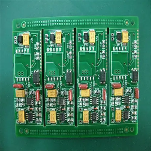
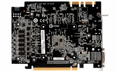
PCBA processing
1. PCB size
PCB width (including board edge) shall be greater than 50 mm and less than 460 mm, and PCB length (including board edge) shall be greater than 50 mm. If the size is too small, it needs to be made into a panel.
2. PCB edge width
Edge width:>5mm, panel spacing:<8mm, distance between pad and edge:>5mm
3. PCB bending
Upward bending degree:<1.2mm, downward bending degree:<0.5mm, PCB twist degree: maximum deformation height ÷ diagonal length<0.25
4. Mark point of PCB
Mark's shape: standard circle, square, triangle;
Mark size: 0.8~1.5mm;
Mark's material: gold plating, tin plating, copper platinum;
Mark's surface requirements: the surface is flat, smooth, free of oxidation and dirt;
Mark's surrounding requirements: there shall be no green oil or other obstacles within 1mm around, which is obviously different from Mark's color;
Mark position: more than 3mm from the edge of the plate, and no holes or test points similar to Mark shall be found within 5mm around.
5. PCB pad
There is no through hole on the bonding pad of SMD components. If there is a through hole, the solder paste will flow into the hole, resulting in less tin in the device, or the tin will flow to the other side, resulting in uneven board surface, and the solder paste cannot be printed.
During PCB production, it is necessary to know some knowledge about PCBA welding process, so as to make products suitable for production. Understanding the requirements of the processing plant first can make the subsequent production and manufacturing process more smooth and avoid unnecessary trouble.
This is the requirement of PCBA welding processing for PCB board. Do not slack off when producing PCB boards. Only by producing high-quality and compliant PCB boards can the boards better accept other special processes, give life to PCB boards, and inject the soul of functions.


Just upload Gerber files, BOM files and design files, and the KINGFORD team will provide a complete quotation within 24h.