
Professional PCB manufacturing and assembly
Building 6, Zone 3, Yuekang Road,Bao'an District, Shenzhen, China
+86-13410863085Mon.-Sat.08:00-20:00

What is the power distribution system on the PCB
Usually, what we show above is<a href="/tw/pcb board. html" target="_self">PCB, the power distribution system (PDS) refers to the subsystem that distributes the power of the Power Source to the devices and devices in the system that need to be powered All power systems have power distribution systems, such as building lighting systems, oscilloscopes, a PCBA, a package, and chips, all of which have internal power distribution systems
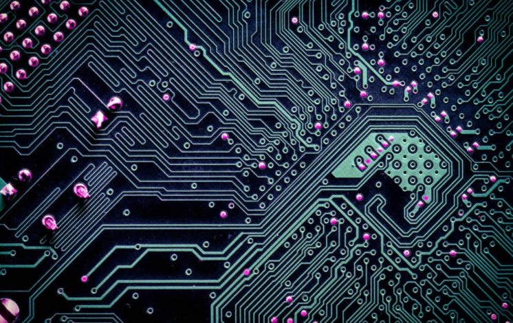
Power distribution system on PCB
In a typical product, the power distribution system includes all interconnections from the voltage regulator module (VRM) toPCB boards, packages and chips. It can be divided into four parts: voltage regulation module (VRM), including its filter capacitor power supply; Bulk capacitors, high-frequency decoupling capacitors, interconnects, vias, power/ground plates on PCB boards - PCB board power distribution system on packages; Packaging pins, connecting wires, interconnects and embedded capacitors - power distribution systems on packages; On chip interconnects, capacitors, etc. - On chip power distribution systems. The so-called power distribution system on the PCB refers to a system on the PCB, which distributes the power supply of the power supply to various chips and devices that need power supply. This paper focuses on the power distribution system on PCB. We agree that the power distribution system or PDS mentioned below refers to the power distribution system on PCB. The function of the power distribution system is to transmit correct and stable voltage, which means that under any load condition, the voltage at all positions on the PCB can be kept correct and stable. The research on the correct and stable operation of distribution system is what we call power integrity.
PCB board

Power integrity
The so-called power integrity refers to the degree to which the system power supply meets the working power supply requirements relative to the equipment port requiring power supply after passing through the power distribution system. Generally speaking, the equipment on the PCB that needs power supply has certain requirements for the working power supply. Taking a chip as an example, it usually displays three parameters: limit power supply voltage: refers to the limit power supply voltage that the chip power supply pin can withstand. The power supply voltage of the chip cannot exceed the required range of this parameter, otherwise the chip may be damaged; In this range, the function of the chip cannot be guaranteed; If the chip is in the limit value of this parameter for a period of time, the long-term stability of the chip will be affected; Recommended working voltage: refers to the range within which the voltage of the chip power supply pin needs to ensure the normal and reliable operation of the chip, usually expressed as "V ± x%", where V is the typical value of the working voltage of the chip power supply pin, and x% is the allowable voltage fluctuation range, and x is usually 5 or 3; Power supply noise: refers to the ripple noise allowed on the chip power supply pin voltage, which enables the chip to work normally and reliably. It is usually represented by its peak to peak value. The data sheet of the chip usually provides the requirements of "limit power supply voltage" and "recommended working voltage". The "power noise" may not be provided separately. In this case, it may be included in the parameter "Recommended operating voltage". "Power Noise" is the focus of this article, which will be discussed separately later. To illustrate with the above example, the power integrity problem is to discuss the "limit power supply voltage" and "recommended working voltage" of the power supply of different power supply pins of the chip relative to the chip pin after the system power passes through the power distribution system. "Power Noise" requirements.
Three characteristics of power distribution system
The physical media of the power distribution system are diverse, including connectors, cables, Trace, power plane, GND plane, Via, Pad, chip pins, etc. Their physical characteristics (data, shape, size, etc.) are different. Since the purpose of the power distribution system is to provide the power supply of the system power supply to the equipment that needs power supply, so as to provide stable voltage and complete current loop, we only pay attention to the three power characteristics of the power distribution system: resistance characteristics, inductance characteristics and capacitance characteristics.
Resistance characteristics
Resistance is a physical quantity representing the resistance of conductor to DC current, usually expressed in R. Its main physical feature is that when the current I flows, it converts electrical energy into thermal energy (I2R) and generates a DC voltage drop (IR) on it. It is a physical property of conductor, which is related to temperature. The resistivity of metal usually increases with temperature. There are resistances everywhere in the power distribution system: there are DC resistances and contact resistances in cables and connectors, distributed resistances in copper wires, power layers, ground planes and vias, and DC impedances in solders, pads and wafer pins. There is contact resistance between them. IR voltage drop: this effect causes the power supply voltage to gradually decrease along the distribution network, or the reference ground voltage to increase, thus reducing the voltage of the equipment port that needs power supply, resulting in power integrity problems; Thermal power dissipation: this effect will reduce the conversion of power supply power into heat, at the same time, it will lead to the rise of system temperature and endanger the stability and reliability of the system. The voltage drop on the RS IRS reduces the output voltage Voutput of the power supply, the voltage drop on the power path IR1 reduces the power supply voltage Vcc of the load, and the voltage drop on the return path IR2 increases the GND level of the load. The voltage drop of the above resistors RS, R1 and R2 will cause the load power supply voltage VCC-GND to decrease, and cause power integrity problems. The heat loss caused by the resistance of the distribution system will cause the power of the power supply to be converted into heat and dissipated in vain, thus reducing the efficiency of the system. At the same time, heating will cause the system temperature to rise, reduce the life of some equipment (such as electrolytic capacitors), thus affecting the stability and reliability of the system. Excessive current density in some areas will also cause local temperature to continue to rise, or even burn out. It can be seen from the above analysis that these two effects are harmful to the system, and their impact is proportional to the resistance value of the resistance. Therefore, one of our design goals is to reduce the resistance characteristics of the distribution system.
Inductance characteristic
Inductance is a physical quantity representing the resistance of conductor to alternating current. When current flows through a conductor, a magnetic field is formed around the conductor. When the current changes, the magnetic field will also change, and the changed magnetic field will form an induced voltage at both ends of the conductor. Voltage polarity will cause induction, and current will hinder the change of original current; When the current change in other conductors around the conductor causes the magnetic field around the conductor to change, the induced voltage will also be generated in the conductor, and the polarity of the voltage will cause the induced current to block the original current. Change. The effect of this conductor on preventing current change is called inductance. The former is called self inductance L, and the latter is called mutual inductance M. Here we directly give two properties of mutual inductance: symmetry: two conductors a and b, regardless of size, shape and relative position, the mutual inductance of conductor a to conductor b is equal to that of conductor b to conductor a, that is, the mutual inductance of two conductors is the same; Mutual inductance is less than self inductance: mutual inductance of any two conductors is less than self inductance of any one conductor. The induced voltage caused by current changes is of great significance to signal integrity (including power integrity), and may lead to transmission line effects, abrupt changes, crosstalk, SSN, track collapse, ground jitter, and most EMI. Inductors are ubiquitous in power distribution systems. Connectors, cables, copper wires, power layers, ground planes, vias, pads, chip pins, etc. have inductances, and mutual inductance exists between adjacent conductors. Suppose that the local self inductance of branch a is La, and the local self inductance of branch b is Lb, the local mutual inductance between the two branches is M, and the current in the loop is I. Since the two branches are parallel, the current flow direction is opposite, and the magnetic field generated by them is opposite. If I is added, for branch a, the polarity of the induced voltage generated by La will prevent the addition of I in branch a, but the polarity of the induced voltage generated by M will help the addition of I in branch a. If branch a represents the power path, branch b represents the return path, Va represents the power noise (rail collapse/power rebound) on the power path, and Vb represents the rail collapse/ground rebound noise on the return path. Both types of noise can cause unstable power supply voltage and lead to power integrity problems. One of our design goals is to reduce the above two voltages. There are two methods: reduce the change rate of the loop current as much as possible: this means that the sudden change rate of the current attracted by the load needs to be reduced, and the number of power ports sharing the power supply path and the return path must be limited; Local mutual inductance between two branches. Reducing the local self inductance of the branch means using the shortest and widest power path and return path as much as possible. The addition of local mutual inductance means that the two branches need to be parallel. It shall be as close as possible under the premise of reverse. From the above analysis, we can see that the induced voltage caused by inductance when the current changes is the root cause of many problems in power supply integrity. In addition, one of our design goals is to reduce the above induced voltage of the distribution system.
Distribution system is the main object discussed in this paper, and the related content of its work is power integrity The distribution system has the characteristics of resistance, inductance and capacitance Resistance and inductance characteristics are harmful to power integrity, while capacitance characteristics are beneficial to power integrity Our design goal is to reduce or even eliminate the influence of resistance and inductance characteristics, and enhance the capacitance characteristics on PCB
How to Select a Reliable PCB Processing Factory
Oct 27,2022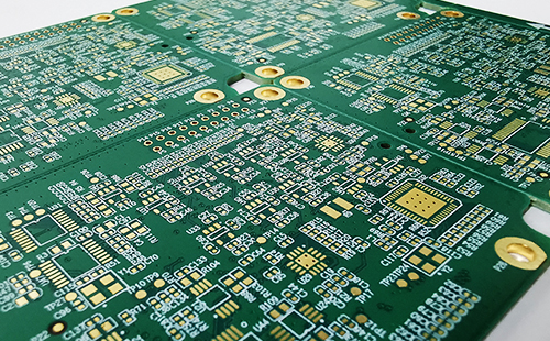


Just upload Gerber files, BOM files and design files, and the KINGFORD team will provide a complete quotation within 24h.