
Professional PCB manufacturing and assembly
Building 6, Zone 3, Yuekang Road,Bao'an District, Shenzhen, China
+86-13410863085Mon.-Sat.08:00-20:00

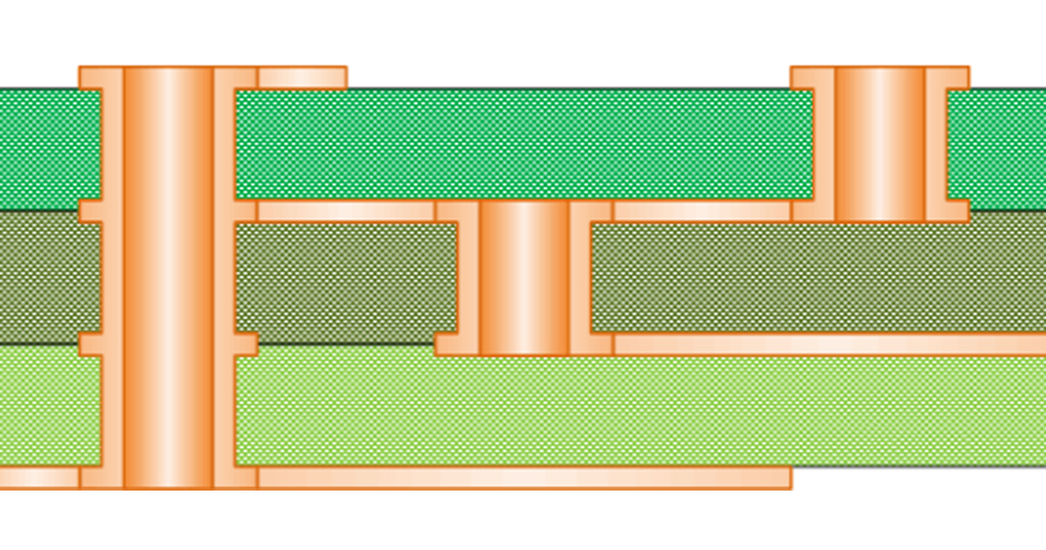
Via is one of the important components of multilayer PCB, and the cost of drilling usually accounts for 30% to 40% of the cost of PCB manufacturing. In short, each hole on a PCB can be called a via.
From the perspective of function, vias can be divided into two categories:
First, it is used as the electrical connection between layers;
Second, it is used for fixing or positioning devices.
In terms of process, these vias are generally divided into three categories, namely blind via, buried via and through via.
1. Blind hole
It is located on the top and bottom surfaces of the printed circuit board and has a certain depth. It is used to connect the surface line and the inner line below. The depth of the hole usually does not exceed a certain ratio (aperture).
2. Buried hole
It refers to the connecting hole in the inner layer of the printed circuit board, which will not extend to the surface of the printed circuit board. The above two types of holes are located in the inner layer of the circuit board. Before lamination, the through hole forming process is used to complete the hole. During the hole forming process, several inner layers may be overlapped.
3. Through-hole
This hole passes through the whole circuit board and can be used for internal interconnection or as the installation positioning hole of components.
Because the through-hole is easier to realize in technology and lower in cost, most printed circuit boards use it instead of the other two kinds of through-hole. The following vias, unless otherwise specified, are considered as through-hole.
From the design point of view, a via is mainly composed of two parts: one is the drill hole in the middle, and the other is the pad area around the drill hole. The size of these two parts determines the size of the vias. Obviously, when designing high-speed and high-density PCBs, the EDA365 Electronic Forum, like the designers, always hopes that the smaller the vias are, the better, so that more wiring space can be left on the board. In addition, the smaller the vias are, the smaller their parasitic capacitance is, which is more suitable for high-speed circuits. However, the reduction of hole size also brings about an increase in cost, and the size of vias cannot be reduced without limitation. It is limited by drilling, plating and other technologies: the smaller the hole, the longer it takes to drill, and the easier it is to deviate from the center; And when the depth of the hole exceeds 6 times of the drilling diameter, it is impossible to ensure that the hole wall can be uniformly copper plated.
For example, if the thickness (through-hole depth) of a normal 6-layer PCB is 50Mil, then under normal conditions, the hole diameter provided by the PCB manufacturer can only reach 8Mil.
With the development of laser drilling technology, the size of drilling can also be smaller and smaller. Generally, vias with a diameter of less than or equal to 6Mil are called micropores. Microholes are often used in HDI (high-density interconnection structure) design. Microhole technology allows vias to be directly punched on the pad (Via in pad), which greatly improves circuit performance and saves wiring space.
The vias on the transmission line behave as breakpoints with discontinuous impedance, which will cause signal reflection. Generally, the equivalent impedance of the vias is about 12% lower than that of the transmission lines. For example, the impedance of a 50 ohm transmission line will decrease by 6 ohm when it passes through the vias (specifically related to the size of the vias and the thickness of the plates, not the reduction).
However, the reflection caused by the discontinuous impedance of the via is actually very small, and its reflection coefficient is only:
(44-50)/(44+50)=0.06
The problems caused by via are more concentrated on the influence of parasitic capacitance and inductance.
1. Parasitic capacitance of via
The via itself has parasitic capacitance to the ground. If it is known that the diameter of the isolation hole of the via on the pavement is D2, the diameter of the via pad is D1, the thickness of the PCB is T, and the dielectric constant of the board substrate is ε, Then the parasitic capacitance of the via is approximate to:
C=1.41 ε TD1/(D2-D1)
Parasitic capacitance of via will mainly affect the circuit by prolonging the rise time of the signal and reducing the speed of the circuit.
For example, for a PCB with a thickness of 50Mil, if a via with an inner diameter of 10Mil and a pad diameter of 20Mil is used, and the distance between the pad and the ground copper area is 32Mil, we can approximately calculate the parasitic capacitance of the via through the above formula:
C=1.41x4.4x0.050x0.020/(0.032-0.020)=0.517pF
The rise time variation caused by this part of capacitance is:
T10-90=2.2C(Z0/2)=2.2x0.517x(55/2)=31.28ps
It can be seen from these values that, although the effect of the rise delay caused by the parasitic capacitance of a single via is not obvious, the EDA365 electronic forum reminds designers to consider carefully if vias are used repeatedly for inter layer switching in routing.
2. Parasitic inductance of via
Similarly, there are parasitic capacitors and parasitic inductors in vias. In the design of high-speed digital circuits, the parasitic inductance of vias often brings more harm than the parasitic capacitance. Its parasitic series inductance will weaken the contribution of bypass capacitor and the filtering effectiveness of the whole power supply system.
We can simply calculate the parasitic inductance of a via approximation using the following formula:
L=5.08h[ln(4h/d)+1]
Where L is the inductance of the via, h is the length of the via, and d is the diameter of the central drilling hole. It can be seen from the formula that the diameter of the via has little influence on the inductance, while the length of the via has little influence on the inductance.
Using the above example, we can calculate the inductance of the via as follows:
L=5.08x0.050[ln(4x0.050/0.010)+1]=1.015nH
If the rise time of the signal is 1ns, the equivalent impedance is:
XL=πL/T10-90=3.19Ω
Such impedance cannot be ignored when there is high-frequency current passing through. In particular, the bypass capacitor needs to pass through two vias when connecting the power layer and the stratum, so the parasitic inductance of the vias will be multiplied.
3. Through Hole Design in High Speed PCB
Through the above analysis of the parasitic characteristics of vias, we can see that in high-speed PCB design, seemingly simple vias often bring great negative effects to circuit design.
In order to reduce the adverse effects caused by the parasitic effect of vias, we can try to do the following in the design:
A. In consideration of cost and signal quality, reasonable size vias are selected. For example, for the 6-10 layer memory module PCB design, it is better to select 10/20Mil (drilling/pad) vias. For some high-density small size boards, you can also try to use 8/18Mil vias.
Under the current technical conditions, it is difficult to use smaller vias. For the via of power supply or ground wire, the larger size can be considered to reduce the impedance.
B. From the two formulas discussed above, it can be concluded that the use of thinner PCB is beneficial to reduce the two parasitic parameters of vias.
C. The pins of power supply and ground shall be punched nearby. The shorter the lead between the via and pin, the better, because they will lead to an increase in inductance. At the same time, the power and ground leads should be as thick as possible to reduce impedance.
D. The signal wiring on the PCB shall not change layers as much as possible, that is to say, unnecessary vias shall be minimized.
E. Place some grounded vias near the vias for signal layer change, so as to provide near circuit for signals. You can even place a large number of redundant grounding vias on the PCB. Of course, the design also needs to be flexible.
The vias model discussed above is the case that each layer has pads. Sometimes, we can reduce or even remove pads from some layers.
Especially when the vias density is very large, it may cause a groove to break the circuit in the copper layer. To solve this problem, in addition to moving the location of vias, we can also consider reducing the pad size of vias in the copper layer.
How to use vias: Through the above analysis of the parasitic characteristics of vias, we can see that in high-speed PCB design, improper use of seemingly simple vias often brings great negative effects to circuit design.

Why pcb board needs positioning and anti dazzle
Oct 25,2022


Just upload Gerber files, BOM files and design files, and the KINGFORD team will provide a complete quotation within 24h.