
Professional PCB manufacturing and assembly
Building 6, Zone 3, Yuekang Road,Bao'an District, Shenzhen, China
+86-13410863085Mon.-Sat.08:00-20:00

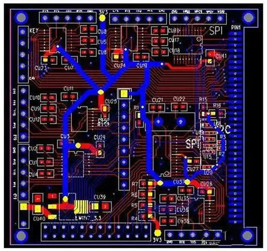
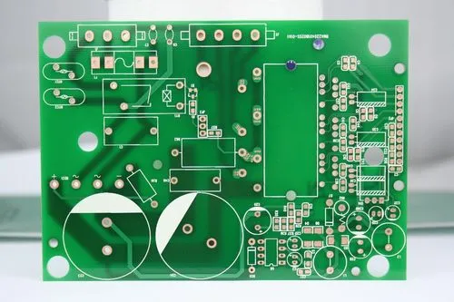
The PCB board is very common in our daily life. If there is a problem, the entire electrical appliance will not be used. So today I will tell you how to inspect the PCB board.
1. PCB board manual visual inspection
Use a magnifying glass or a calibrated microscope, and use the operator's visual inspection to determine if the circuit board is unqualified, and determine when the correction operation is required.
Advantages: low pre cost and no test fixture;
Disadvantages: At present, due to the increase of PCB output and the reduction of PCB wire spacing and component volume, this method becomes more and more infeasible;
2. PCB board online test
To find out manufacturing defects and test analog, digital and mixed signal PCB components through electrical performance testing to ensure that they meet the specifications, there are several testing methods such as needle bed tester and flying needle tester.
Advantages: low test cost of each board, strong digital and functional test capability, fast and thorough short circuit and open circuit test, programming firmware, high defect coverage and easy programming.
Disadvantages: It requires testing fixture, programming and debugging time, high cost of making fixture, and difficult to use.
3. PCB board function test
Functional system test is to use special test equipment at the middle and end of the production line to comprehensively test the functional modules of the circuit board to confirm the quality of the circuit board.
4. Automatic optical inspection
Also known as automatic visual inspection, it is a new method to identify manufacturing defects based on optical principles, using image analysis, computer, automatic control and other technologies to detect and process defects encountered in production.
5. Automatic X-ray inspection
Defects are found in the parts to be inspected by fluoroscopy based on the different absorptivity of different substances to X-ray. It is mainly used to detect defects such as bridging, chip loss, and poor alignment caused by ultra-fine spacing, ultra-high density circuit boards, and PCB assembly process. It can also use its tomography technology to detect internal defects of IC chips. It is the only way to test the welding quality of the ball grid array and the shielded solder balls.
Advantages: BGA welding quality and embedded components can be detected, and internal conditions of high-precision products can be detected;
Disadvantages: high cost;
6. Laser detection system
It is the latest development of PCB technology. It uses a laser beam to scan the printed circuit board, collect all measured data, and compare the actual measured value with the preset qualified limit value. This technology has been verified on the light plate, and is being considered for assembly plate testing. The speed is enough for mass production lines.
Advantages: fast output, no need for clamps and visual non masked access;
Disadvantages: high initial cost, maintenance and use problems are the main disadvantages.


Just upload Gerber files, BOM files and design files, and the KINGFORD team will provide a complete quotation within 24h.