
Professional PCB manufacturing and assembly
Building 6, Zone 3, Yuekang Road,Bao'an District, Shenzhen, China
+86-13410863085Mon.-Sat.08:00-20:00


In daily life, the application of circuit board is very common. The electronic products that can be contacted by us will be applied to the circuit board. Opening the inner liner of all electronic products, we finally found that such a small circuit board is expected to support the work of electronic products. However, due to the extensive use of circuit boards, consumers and businesses have higher requirements for the production materials and processes of circuit boards, at this time, printed circuit boards came into being. Next, let's take a look at the whole process of PCB.
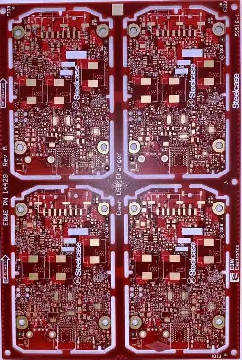
Printed circuit board products
If you want to produce and this year's printed PCB products, you should first design the schematic according to the function of the circuit. The schematic should be built according to the electrical functions and needs of each part. The completed design schematic can perfectly reflect the main functions of the PCB and strengthen the connection between each part. After this step is completed, install the software that has been placed so that all components and devices have the same specifications and dimensions. After the packaging is completed, the sealing of the device shall be checked according to the inspection rules. After that, use special carbon paper to print the approved bcd drawings through the inkjet printer, and then put the printed copper paper in the solution prepared by sulfuric acid and hydrogen oxide. After all the ink is removed, clean the copper plate with clean water. Finally, it is necessary to use a drilling machine to drill holes on the circuit board where the holes need to be drilled. After all welding work is completed, the entire printed circuit board will be completely inspected and verified again. After all these work is completed, all work on the printed circuit board will be completed.
After talking about all the processes of PCB production, we can clearly know that PCB is replacing the electronic PCB with complicated production processes. Compared with the traditional electronic circuit board, it not only shortens the production cycle of a single circuit board, but also has greater advantages in production cost and quality.
Manufacturing process of PCB
PCB is widely used in various electronic products. Any PCB product can not be separated from the installation and use of PCB. In these electronic products, we need certain PCB to ensure the normal operation of an electronic product.
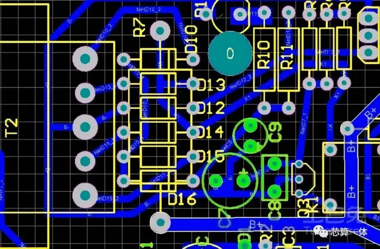
Circuit board
Then our PCBs are also classified into three categories according to the number of orders: single-sided and double-sided PCBs and multilayer PCBs. The threads are concentrated on one side and on the other side, especially on the parts of the assembled PCB. From this point of view, this is just a thread, and the terminal of this PCB is called. They are usually simple, and the manufacturing cost of the board on one side is low, and they are not used, and the disadvantages of the new product are too complex.
The extension of the double-sided board is on one side. When PCB single-layer wiring cannot meet the needs of electronic products, double-sided circuit boards shall be used. The lines in the air are put on the clothes, and they pass through the holes on both sides. Through them, the battle line and the network that can form between them become necessary. Multilayer board refers to printed board model. These three orders are to stack more conductive and insulating conductive materials at certain intervals and for reasons of interconnection. One is to make mistakes. Multilayer electronic multi round development products in the Arabic Department office are attracted to smaller or smaller members.
Due to the small size and complex structure of the circuit board, it is necessary to use special observation equipment to observe the circuit board. Usually, the mobile video microscope is used to observe the structure of the circuit board, but through the video microscope, the circuit sensitive microscope can be clearly seen from the microscope. This makes it easier to design and test circuit boards.
These PCB manufacturing processes are definitely not some products that can be produced in a short time. They can only be formally produced after a series of design and research. Because these PCB are also a key means of electronic products, the manufacturing process of PCB is really a bit complicated.


Just upload Gerber files, BOM files and design files, and the KINGFORD team will provide a complete quotation within 24h.