
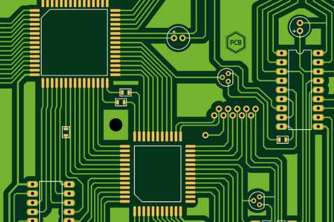
Professional PCB manufacturing and assembly
Building 6, Zone 3, Yuekang Road,Bao'an District, Shenzhen, China
+86-13410863085Mon.-Sat.08:00-20:00

If wiring doesn't require extra layers, why bother with it? Wouldn't fewer layers make the board thinner? If the board is one layer less, isn't the cost lower? However, in some cases, adding an additional layer may actually reduce the cost.
Because there is one less layer of media and coating foil, the cost of odd-numbered PCB board raw materials is slightly lower than that of even-numbered PCB. However, the processing cost of odd-layer PCB is significantly higher than that of even-layer PCB. The processing cost of the inner layer is the same; However, the foil/core structure significantly increases the processing cost of the outer layer.
Odd-layer PCB needs to add a non-standard laminated nuclear layer bonding process on the basis of the nuclear structure process. Compared with the nuclear structure, the production efficiency of the factory where PCB proofing adds foil outside the nuclear structure will decrease. Before laminate bonding, the outer core requires additional processing, which increases the risk of scratches and etched errors on the outer layer
.
Balanced structure to avoid bending
The best reason not to design a PCB with odd layers is that odd-layer boards are easy to bend. When the PCB is cooled after the multi-layer circuit bonding process, the different lamination tension when the core structure and the foil structure are cooled will cause the PCB to bend. As the board thickness increases, the risk of bending a composite PCB with two different structures increases. The key to eliminating circuit board bending is to use balanced layering. Although the PCB with a certain degree of bending meets the requirements of the specification, the subsequent processing efficiency will be reduced, resulting in an increase in costs. Because special equipment and processes are required during assembly, the accuracy of component placement is reduced, so the quality will be compromised.
PCB circuit board short circuit several inspection methods
First, open the PCB design drawing on the computer, light up the short-circuit network, and see what place is closest and most easily connected to a piece. Pay special attention to the short circuit inside the IC.

Second, if it is manual welding, to develop good habits:
1, before welding to visually check the PCB board, and use a multimeter to check the key circuit (especially power and ground) is short circuit;
2, each time after welding a chip, use a multimeter to test whether the power supply and ground short circuit;
3, do not toss the soldering iron when welding, if the solder is thrown to the welding foot of the chip (especially the sticker components), it is not easy to find.
Three, found a short circuit phenomenon. Take a board to cut the line (especially suitable for single/double board), after cutting the line, each part of the function block is powered separately, and gradually eliminated.
Fourth, if there is a BGA chip, because all the solder joints are covered by the chip can not be seen, and it is a multi-layer board (more than 4 layers), so it is best to split the power supply of each chip at the time of design, with magnetic beads or 0 ohmresistance connection, so that when the power supply and the ground short circuit, disconnect the magnetic bead detection, it is easy to locate a chip. Due to the difficulty of BGA welding, if it is not automatically welded by the machine, a little attention will short-circuit the adjacent power supply and the two welding balls.
Five, small size of the surface capacitor welding must be careful, especially the power filter capacitor, the number is large, it is easy to cause short circuit between the power supply and the ground. Of course, sometimes bad luck will encounter that the capacitor itself is short-circuited, so the best way is to detect the capacitor before welding.
Advantages and disadvantages of different surface treatments of PCB boards
There are many types of surface treatment of the circuit board, PCB proofing personnel should choose according to the performance and needs of the board, the following simple analysis of the advantages and disadvantages of various surface treatment in PCB manufacturing for reference!
1 HASL hot air smoothing (we often say tin spraying)
Tin spraying is a common treatment for PCB in the early days. It is now divided into lead spray tin and lead-free spray tin.
Advantages of spray tin:
Long storage time
After the PCB is finished, the copper surface is completely wet (completely covered with tin before welding).
Suitable for lead-free welding
Process maturity
Low cost
Suitable for visual inspection and electrical measurement
Weaknesses of tinspray:
Not suitable for wire binding; Due to surface flatness problems, there are also limitations on SMT; Not suitable for contact switch design.
The copper dissolves when the tin is sprayed and the board is subjected to a high temperature.
Especially thick or thin plate, the spray tin is limited, the production operation is not convenient.
2 OSP (Organic Protective Film)
The process is simple and the surface is very flat, suitable for lead-free welding and SMT.
Easy to rework, convenient production operation, suitable for horizontal line operation.
Suitable for multiple processing on the board (e.g. OSP+ENIG)
Low cost, environmentally friendly.
OSP weaknesses:
Limit the number of reflux times (multiple welding thick, the film will be destroyed, basically 2 times no problem)
Not suitable for crimp technology, wire binding.
Visual detection and electrical detection are not convenient.
N2 gas protection is required for SMT.
SMT rework is not suitable.
High storage requirements.
3 Chemical silver
Chemical silver is a better surface treatment process.
Advantages of chemical silver:
Simple process, suitable for lead-free welding, SMT.
Very flat surface
Suitable for very fine lines.
Low cost.
Chemical silver's weaknesses:
High storage requirements, easy to pollute.
Welding strength is prone to problems (micro-cavity problem).
It is easy to have electromigration phenomenon and Javani bite phenomenon of copper under welding resistance film.
Electrical measurement is also a problem


Just upload Gerber files, BOM files and design files, and the KINGFORD team will provide a complete quotation within 24h.