
Professional PCB manufacturing and assembly
Building 6, Zone 3, Yuekang Road,Bao'an District, Shenzhen, China
+86-13410863085Mon.-Sat.08:00-20:00

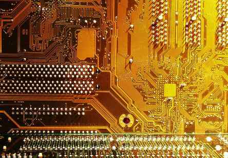
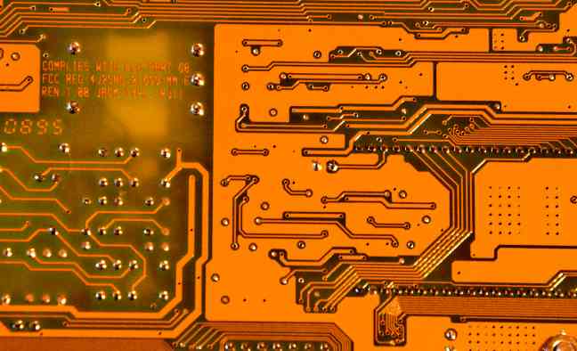
The transmission rate of high-speed PCB designwiring system is steadily accelerating, but also brings some anti-interference vulnerability, because the higher the frequency of transmission information, the sensitivity of the signal increases, and their energy is weaker and weaker, the more susceptible the wiring system is to interference.
Interference is ubiquitous, and cables and equipment can interfere with other components or be seriously interfered with by other sources of interference, such as: computer screens, mobile phones, electric motors, radio relay equipment, data transmission and power cables. In addition, the number of potential eavesdroppers, cybercriminals and hackers is increasing because their interception of UTP cable information transmission can cause great damage and loss.
Especially when using high-speed data networks, the time required to intercept large amounts of information is significantly lower than the time required to intercept low-speed data transmission. The stranded pair in the data twisted pair can rely on its own stranded to resist external interference and crosstalk between the pair at low frequency, but in the case of high frequency (especially when the frequency exceeds 250MHz), only the stranded pair can not achieve the purpose of anti-interference, only the shield can resist external interference.
The cable shield acts like a Faraday shield, and the interference signal will enter the shield but not the conductor. As a result, data transmission can run without trouble. Because the shielded cable has a lower radiation emission than the unshielded cable, the network transmission is prevented from being intercepted. Shielding networks (shielded cables and components) can significantly reduce the level of electromagnetic energy radiation entering the surrounding environment that can be intercepted.

Different interference field shielding selection interference field mainly has electromagnetic interference and radio frequency interference two kinds. Electromagnetic interference (EMI) is mainly low-frequency interference, and motors, fluorescent lamps and power cords are the usual sources of electromagnetic interference. Radio frequency interference (RFI) refers to radio frequency interference, mainly high frequency interference. Radio, television, radar and other wireless communications are common sources of RF interference.
To resist electromagnetic interference, braided shielding is the most effective because of its low critical resistance. For RF interference, foil shielding is the most effective, because braided shielding depends on the change of wave length, and the gap generated by braided shielding allows high-frequency signals to enter and exit the conductor freely. For the high and low frequency mixed interference field, it is necessary to adopt the combination of foil layer and braided net with broadband coverage function. Generally, the higher the mesh shielding coverage, the better the shielding effect.
1, 3 points above the line, try to make the line through each point, easy to test, the line length as short as possible.
2, try not to put wires between pins, especially between and around integrated circuit pins.
3, the lines between different layers should not be parallel as far as possible, so as not to form an actual capacitor.
4, the wiring is as straight as possible, or 45 degree line, to avoid electromagnetic radiation.
5, ground wire, power cord at least 10-15mil above (for logic circuit).
6. Try to connect the ground polysemy lines together and increase the ground area. Line to line as neatly as possible.
7, pay attention to the uniform emission of components, so as to install, plug-in, welding operation. The text is discharged in the current character layer, the position is reasonable, pay attention to the orientation, avoid being blocked, easy to produce.
8, the component emission should consider the structure, and the positive and negative electrodes of the patch components should be marked in the package and at the end to avoid space conflicts.
9, the current printed board can be used for 4-5mil wiring, but usually 6mil line width, 8mil line distance, 12/20mil pad. Wiring should consider the influence of the input current.
10. Put the functional block components together as far as possible, and the components near the LCD such as zebra strips can not be too close.
11, through the hole to paint green oil (set to negative double value).
12, it is best not to place the PAD under the battery holder, over empty, etc., PAD and VIL size is reasonable.
13, after the wiring is completed, carefully check whether each connection (including NETLABLE) is really connected (available lighting method).
14, the oscillating circuit components as close as possible to the IC, the oscillating circuit as far as possible away from the antenna and other vulnerable areas. Put a ground pad under the crystal oscillator.
15, consider strengthening, hollowing out elements and other ways to avoid excessive radiation sources.


Just upload Gerber files, BOM files and design files, and the KINGFORD team will provide a complete quotation within 24h.