
Professional PCB manufacturing and assembly
Building 6, Zone 3, Yuekang Road,Bao'an District, Shenzhen, China
+86-13410863085Mon.-Sat.08:00-20:00

DIP dual in-line packaging process
With the rapid development of SMT processing technology, SMT patch processing has gradually replaced DIP insertion processing. However, due to the oversize of some electronic components in PCBA production and other reasons, plug-in processing has not been replaced and still plays an important role in the electronic assembly process.
Before entering the topic, in order to help readers better understand the article, it is necessary to explain some nouns first.
1. SMT: the abbreviation of Surface Mounted Technology, refers to the surface assembly technology (surface mount technology), which is the most popular technology and process in the electronic assembly industry;
2. PCBA: the abbreviation of Printed Circuit Board Assembly, which is the whole process of PCB empty board assembled by SMT upper part or DIP plug-in, referred to as PCBA;
3. PCB: The abbreviation of Printed Circuit Board. The Chinese name is printed circuit board, also known as printed circuit board. It is an important electronic component, a support for electronic components, and an important carrier for electrical interconnection of electronic components. Because it is made by electronic printing, it is called "printed" circuit board; Note: PCBA generally refers to a processing process, which can also be understood as a finished circuit board, that is, after the processes on the PCB are completed Can be counted as PCBA. The PCB refers to an empty printed circuit board with no parts on it. It can be simply understood as: PCBA is a finished board, and PCB is a bare board.
4. THT: The abbreviation of Through Hole Technology, which refers to the through-hole technology that inserts components into the circuit board and then solders them firmly with solder (traditional through-hole insertion technology); 5. DIP: dual in-line package The acronym refers to dual in-line packaging, which is a packaging method for integrated circuits.
Historical development of DIP
The earliest DIP packaging components were invented by Bryant Buck Rogers of Fairchild Semiconductor in 1964. The first components had 14 pins, which were quite similar to today's DIP packaging components. Its shape is rectangular. Compared with earlier round components, rectangular components can increase the density of components in the circuit board.
DIP packaged components were the mainstream of the microelectronics industry in the 1970s and 1980s. In the 1990s, components with more than 20 pins may still have DIP packaged products. In the 21st century, many new programmable components are packaged in SMT, and products in DIP package are no longer available.
DIP belongs to THT
THT uses leaded components, design the circuit connection wires and mounting holes on the printed board, insert the component leads into the pre-drilled through holes on the PCB, temporarily fix them on the other side of the substrate by wave soldering and other soft Brazing technology is used for welding to form reliable solder joints and establish long-term mechanical and electrical connections. The main body of components and solder joints are distributed on both sides of the substrate. With this method, since the components have leads, when the circuit is dense to a certain extent, the problem of reducing the size cannot be solved. At the same time, it is difficult to eliminate the faults caused by the proximity of the leads and the interference caused by the length of the leads.
DIP packaging (DualIn-linePackage) is a component packaging technology in the THT plug-in process, and it is the simplest packaging method. Most small and medium-scale integrated circuits use this package, and the number of pins generally does not exceed 100. The DIP-packaged CPU chip has two rows of pins and needs to be inserted into a chip socket with a DIP structure.
DIP production process

The DIP production process can be divided into seven steps: component molding, plug-in, wave soldering, component cutting (cutting) feet, repair soldering, board washing and functional testing:
1. Pre-processing the components. First of all, the staff in the pre-processing workshop go to the material place to pick up the materials according to the material list, carefully check the material model, specification, sign, and carry out pre-production pre-processing according to the model, using automatic bulk capacitor cutting machine, transistor automatic molding machine, automatic belt Forming equipment such as type forming machines for processing;
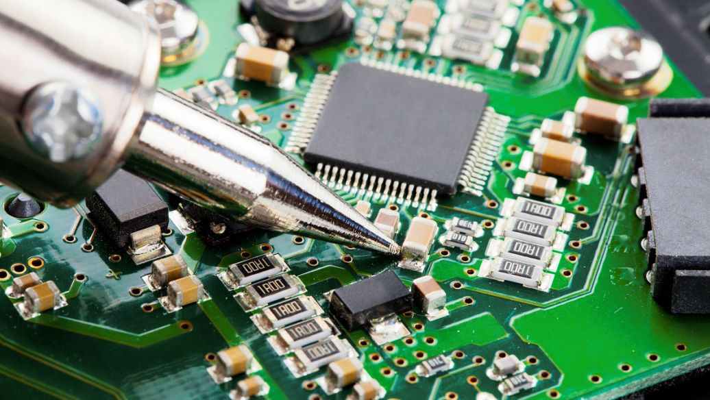
2. Plug-in, inserting the processed components into the corresponding position of the PCB board to prepare for wave soldering;
manual plug-in
3. Wave soldering, put the plug-in PCB board into the wave soldering conveyor belt, and complete the soldering of the PCB board after spraying flux, preheating, wave soldering, cooling and other links;
Component cut foot
4. Cut (cut) the feet of the components, and cut (cut) the feet of the soldered PCBA board to achieve the appropriate size;
5. Repair welding (post-welding), for PCBA finished boards that are not completely welded after inspection, repair welding should be carried out for maintenance;
repair welding
6. Wash the board, clean the harmful substances such as flux remaining on the finished PCBA, so as to meet the cleanliness of the environmental protection standard required by the customer;
7. Functional test. After the components are soldered, the finished PCBA board needs to be functionally tested to check whether each function is normal. If a functional defect is detected, it needs to be repaired and retested.
Introduction to DIP equipment
Automatic plug-in machine
Principle: According to the program setting, the materials are sequentially loaded on the automatic plug-in machine. After the PCB is positioned, the suction head absorbs the parts and detects the size and type of the parts according to the part specifications set by the program, and then mounts them sequentially according to the placement coordinates. On the position of the parts required by the PCB.
Automatic plug-in machine
Wave Soldering Machine
Wave soldering is to form a solder wave of a specific shape (fish scale-like ripples on the surface of the solder seam) on the liquid surface of the solder tank with the help of the molten liquid solder and the action of the pump, and place the PCB with the components inserted on the conveyor chain. The process of soldering through the solder wave at a specific angle and a certain depth of immersion to achieve solder joints.
PCB board flow into wave soldering
Precautions for DIP processing
1. Before plugging in, check whether there are oil stains, paint and other unclean objects on the surface of electronic components.
2. During the plug-in process, it is necessary to ensure that the electronic components and the PCB are flat. After the plug-in is completed, the electronic components must be in a flat state.
3. If there is a direction indicator on the electronic component, it must be plugged in the correct direction, and do not plug in at will.
4. When plugging in, pay attention to the force of the plug-in. Do not use too much force when plugging in, which will cause damage to components or damage to the PCB board.
5. Do not insert the edge of the PCB board when inserting electronic components, pay special attention to the height of electronic components and the distance between electronic components.


Just upload Gerber files, BOM files and design files, and the KINGFORD team will provide a complete quotation within 24h.