
Professional PCB manufacturing and assembly
Building 6, Zone 3, Yuekang Road,Bao'an District, Shenzhen, China
+86-13410863085Mon.-Sat.08:00-20:00


Electro Magnetic Compatibility (EMC) is a new comprehensive subject, it mainly studies electromagnetic interference and anti-interference problems. Electromagnetic compatibility means that electronic equipment or system does not reduce the performance index due to electromagnetic interference under the specified electromagnetic environment level, and the electromagnetic radiation generated by them is not greater than the limited limit level, so as to not affect the normal operation of other systems, and achieve the purpose of non-interference between equipment and equipment, and between systems, and common reliable work.
Electromagnetic interference (EM I) is caused by the electromagnetic interference source to transfer energy to the sensitive system through the coupling path, which includes three basic forms: conduction by wire and common ground, through space radiation or near field coupling. Practice has proved that even if the Circuit schematic design is correct and the Printed circuit Board is improperly designed, it will have an adverse effect on the reliability of electronic equipment, so ensure the electromagnetic compatibility of the printed circuit board is the key to the entire system design. This paper mainly discusses the electromagnetic compatibility technology and printed circuit board (Printed Circuit Board, printed circuit board, printed circuit board, printed circuit board, printed circuit board, PCB) in the design of the application.

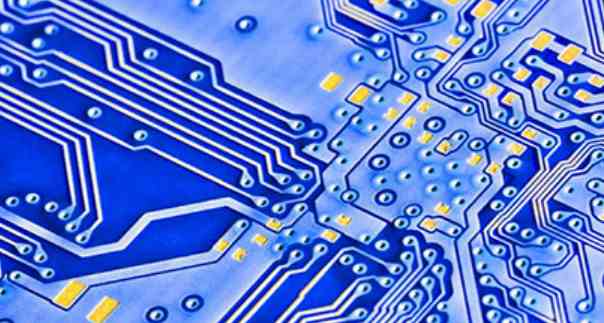
PCB is the support parts of circuit components and devices in electronic products. It provides the electrical connection between circuit components and devices. It is the most basic component of various electronic equipment. Nowadays, large-scale and ultra-large scale integrated circuits have been widely used in electronic equipment, and the installation density of components on printed circuit boards is getting higher and higher, and the transmission speed of signals is getting faster and faster. EMC problems caused by this become more and more prominent. PCB has a single panel (single layer board), double panel (double layer board) and multilayer board. Single and dual panels are generally used for circuits with low and medium density wiring and circuits with low integration, while multilayer panels use high density wiring and circuits with high integration. From the perspective of electromagnetic compatibility, single panel and double panel are not suitable for high speed circuit, single side and double side wiring can not meet the requirements of high performance circuit, and the development of multi-layer wiring circuit provides a possibility to solve the above problems, and its application is becoming more and more widespread.
1. Characteristics of multi-layer wiring
PCB is composed of organic and inorganic dielectric materials with multilayer structure. The connection between layers is realized through holes, which can be plated or filled with metal materials to achieve electrical conduction between layers. The reason why multilayer wiring is widely used is that there are the following characteristics:
(1) The multi-layer board is provided with a special power layer and ground layer. The power layer can be used as a noise loop to reduce interference; At the same time, the power layer also provides a loop for all the system signals, eliminating the common impedance coupling interference. The impedance of the power supply line is reduced, thus reducing the public impedance interference.
(2) The multi-layer board adopts a special ground layer, which has a special ground wire for all signal lines. The characteristic of signal line: the impedance is stable and easy to match, reducing the waveform distortion caused by reflection; At the same time, a special ground layer is used to increase the distributed capacitance between the signal line and the ground line, and reduce the crosstalk.
2. Laminated design of printed circuit board
2. Wiring rules of 1PCB
The EMC analysis of multilayer circuit boards can be based on Kirchhoff's law and Faraday's law of electromagnetic induction. According to Kirchhoff's law, the transmission of any time-domain signal from source to load must have a path with the lowest impedance.
PCBS with multiple layers are often used in high-speed, high-performance systems, where the multiple layers are used for direct current (DC) power supplies or ground reference planes. These planes are usually solid planes without any division, because there are enough layers to be used as power sources or strata, so there is no need to place different DC voltages on the same layer. This layer will be used as a current return path for signals on the transmission lines adjacent to them. Constructing a low impedance current return path is the most important EMC goal for these planar layers.


Just upload Gerber files, BOM files and design files, and the KINGFORD team will provide a complete quotation within 24h.