
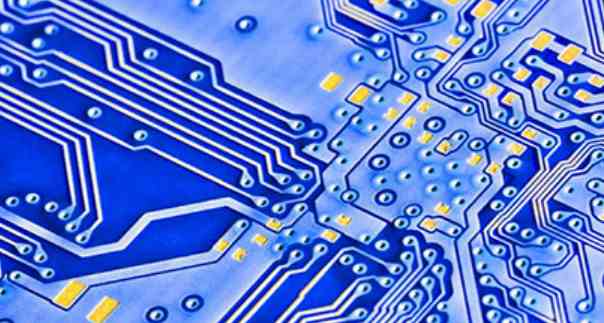
Professional PCB manufacturing and assembly
Building 6, Zone 3, Yuekang Road,Bao'an District, Shenzhen, China
+86-13410863085Mon.-Sat.08:00-20:00


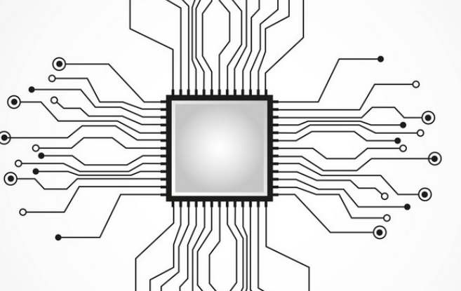
The significance of PCB design of various boards:
toplayer - the top wiring layer.
bottomlayer - The bottomlayer of wiring, which has electrical characteristics. It is the wiring on the circuit board that connects the pins of each component.
mechanical -- the mechanical layer is what defines the appearance of the whole PCB board, actually when we say the mechanical layer we mean the structure of the whole PCB board.
keepoutlayer - No wiring layer. The No wiring layer is the boundary that defines the electrical characteristics of copper we lay. That is to say, after we define no wiring layer first, it is not possible to lay wires with electrical characteristics beyond the boundary of no wiring layer in the future wiring process.
topoverlay -- top screen printing layer.
bottomoverlay -- the bottom screen layer, defining the top and bottom screen characters, which are the component numbers and some characters that you typically see on a PCB board.
toppaste -- the top layer of the pad.
The bottompaste -- the bottom pad, the top layer and the bottom pad, which is the pad that you can see the patch element on.
topsolder -- topsolder layer.
bottomsolder -- the bottomsolder layer. Because the PCB board is to be coated with green oil by default, a "skylight" will be opened where you draw the line with these two layers, so that you won't get green oil. It can be used in places where large currents are needed to add additional solder.
The multilaye layer is actually similar to the mechanical layer. As the name suggests, this layer refers to all the layers of the PCB board
Backward crosstalk occurs for the same physical reason as forward crosstalk: the time-varying electric and magnetic fields of the "intrusive" signal cause the inductive and capacitive signals in the "victim". But there are differences between the two.

The biggest difference is the duration of the backward crosstalk signal. Because the forward crosstalk and the "intrusion" signal travel in the same direction and speed, the duration of the forward crosstalk is the same length as the "intrusion" signal. However, the backward crosstalk and the "intrusion" signal travel in the opposite direction, it lags behind the "intrusion" signal and causes a long series of pulses.
Unlike forward crosstalk, the amplitude of the backward crosstalk pulse is independent of line length, and the duration of the pulse is twice as long as the delay time of the "intrusive" signal. Why? Suppose you look at the backward crosstalk from the point of departure of the signal. When the "intrusive" signal is away from the point of departure, it is still producing the backward pulse until another delayed signal appears. Thus, the entire duration of the backward crosstalk pulse is twice as long as the delay time of the "intrusive" signal.
3. Backward crosstalk reflection
You probably don't care about crosstalk interference on the driver and receiver chips. However, why should you care about the backward pulse? Because the driver chip generally has a low resistance output, it reflects more crosstalk signals than it absorbs. When the backward crosstalk signal reaches the driver chip of the "victim", it is reflected back to the receiving chip. Because the output resistance of the driver chip is generally lower than the wire itself, it often causes the reflection of crosstalk signal.
Unlike forward crosstalk signals, which are both sensitive and capacitive, backward crosstalk signals have only one polarity, so they cannot cancel themselves out. The backward crosstalk signal and its reflected crosstalk signal have the same polarity as the "intrusive" signal, and their amplitude is the sum of the two parts.
Remember, when you detect a backward crosstalk pulse at the receiving end of the victim, the crosstalk signal has already been reflected by the victim driver chip. You can observe that the polarity of the backward crosstalk signal is the opposite of the "intrusion" signal.
In digital design, you often care about quantitative metrics such as the maximum noise tolerance of 150mV regardless of how and when the crosstalk is produced, forward or backward. So, is there a simple way to measure noise accurately? The short answer is "no," because electromagnetic field effects are too complex, involving a series of equations, the topology of the circuit board, the simulation characteristics of the chip, and so on.
From a practical point of view, the most important problem is how to remove crosstalk. What do you do when crosstalk affects circuit characteristics?
There are two strategies you can take. One approach is to vary one or more geometric parameters that affect coupling, such as line length, distance between lines, and layering position of the board. Another approach is to use a terminal, replacing a single line with a multiplex coupled line. Properly designed, multi-wire terminals can cancel most crosstalk.


Just upload Gerber files, BOM files and design files, and the KINGFORD team will provide a complete quotation within 24h.